Ceramic block side wall printing method
A printing method and a technology for ceramic blocks, which are applied to the formation of conductive patterns and other directions, can solve the problems of affecting quality, low work efficiency, and high production costs, and achieve the effects of reducing production costs, good printing quality, and improving work efficiency.
- Summary
- Abstract
- Description
- Claims
- Application Information
AI Technical Summary
Problems solved by technology
Method used
Image
Examples
Embodiment Construction
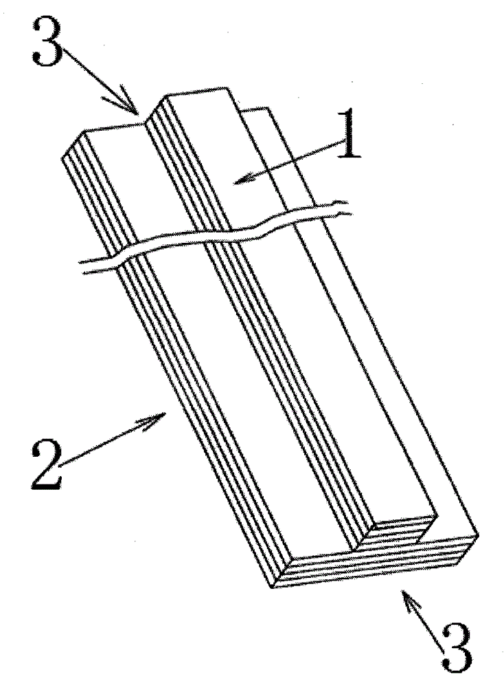
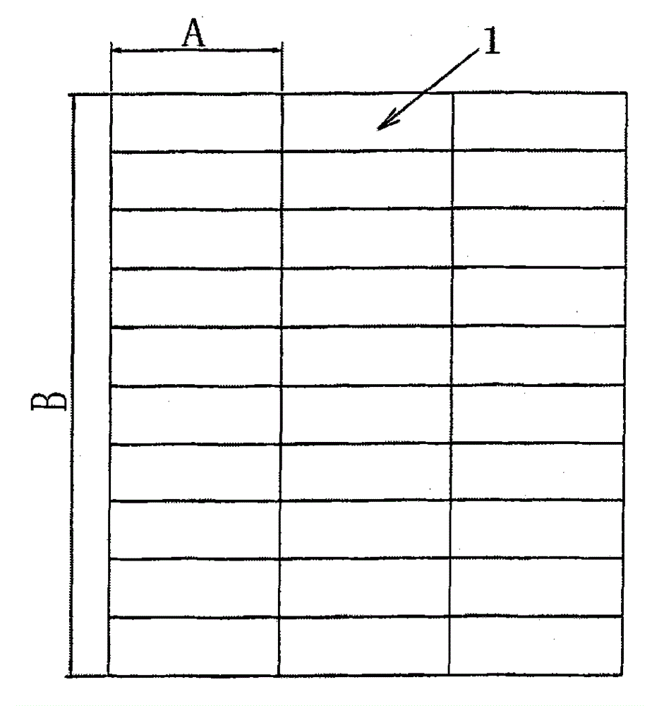
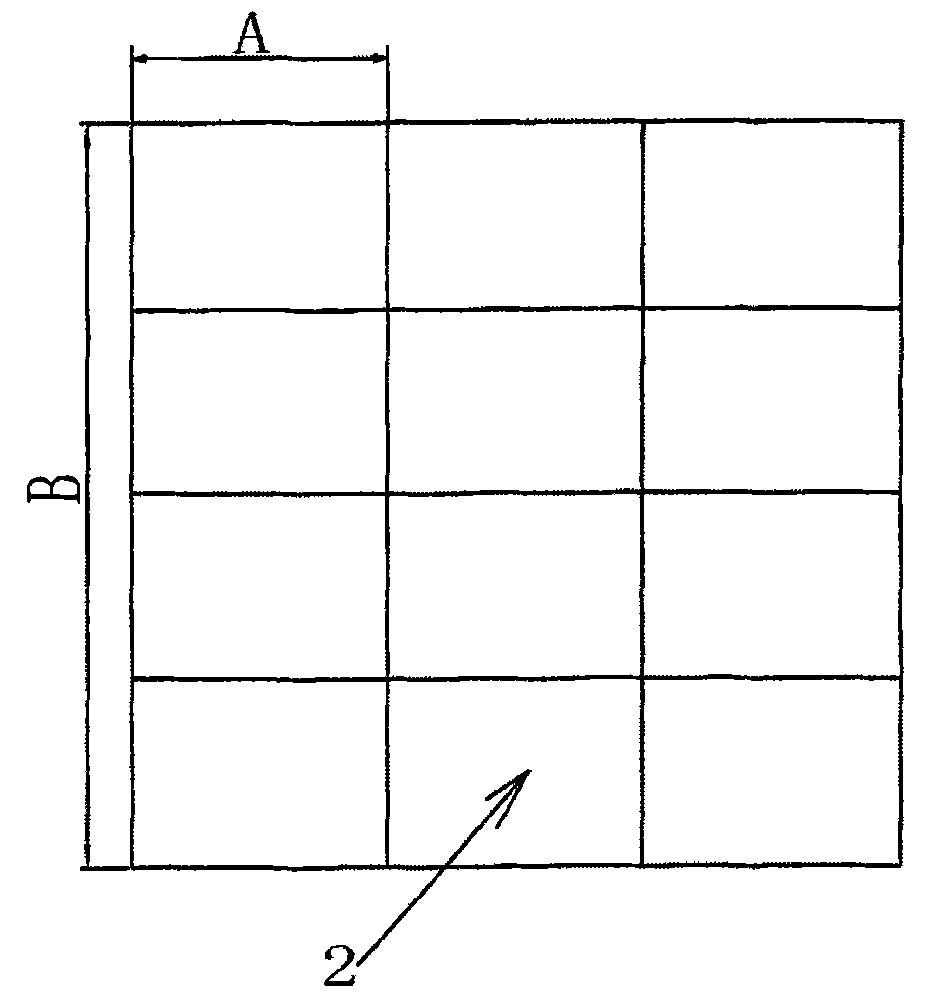
[0015] As shown in the figure: follow the steps below:
[0016] a. Before stacking the four-layer ceramic substrates together, use screen printing to print metal paste on the top surface of the uppermost ceramic substrate, and use the same method to print the metal paste on the bottom ceramic substrate of another group of four-layer ceramic substrates. The metal paste is printed on the bottom surface, that is, a single ceramic substrate is printed, and then the four layers are laminated together.
[0017] b. Laminate the four-layer ceramic substrate printed in the previous step by using the usual lamination technology to make it a whole.
[0018] c. Cut off the edges and corners of the board laminated in the previous step to form a rectangle. According to the length and width of the ceramic substrate, determine that the width A of the rectangle is consistent with the length of the ceramic block, and the length B of the rectangle is the width of the upper ceramic block 1. Inte...
PUM
 Abstract
Description
Claims
Application Information
 - Generate Ideas
- Intellectual Property
- Life Sciences
- Materials
- Tech Scout
- Unparalleled Data Quality
- Higher Quality Content
- 60% Fewer Hallucinations
Browse by: Latest US Patents, China's latest patents, Technical Efficacy Thesaurus, Application Domain, Technology Topic, Popular Technical Reports.
© 2025 PatSnap. All rights reserved.Legal|Privacy policy|Modern Slavery Act Transparency Statement|Sitemap|About US| Contact US: help@patsnap.com


