
Groove type CoolMOS and manufacturing method thereof

A manufacturing method and trench-type technology, which are applied in semiconductor/solid-state device manufacturing, electrical components, circuits, etc., can solve the problems of reducing process steps, complex CoolMOS manufacturing process, and reducing chip area, so as to reduce chip area and manufacturing Steps to improve the effect of pressure resistance

Inactive Publication Date: 2016-08-17
SUZHOU TONGGUAN MICROELECTRONICS
View PDF4 Cites 8 Cited by
  • Summary
  • Abstract
  • Description
  • Claims
  • Application Information

AI Technical Summary

Problems solved by technology

[0004] The purpose of the present invention is to overcome the defects of the complex manufacturing process of CoolMOS in the prior art, and provide a trench-type CoolMOS and its preparation method, which adopts the process of back digging and filling P-type silicon, so as to achieve multiple implantation and diffusion of P-type ions The effect; the trench gate structure is adopted on the front side, which reduces the process steps, reduces the chip area, saves equipment and production costs, and improves the electrical performance of the device

Method used


Image

  • Groove type CoolMOS and manufacturing method thereof
  • Groove type CoolMOS and manufacturing method thereof
  • Groove type CoolMOS and manufacturing method thereof

Examples


Embodiment 1

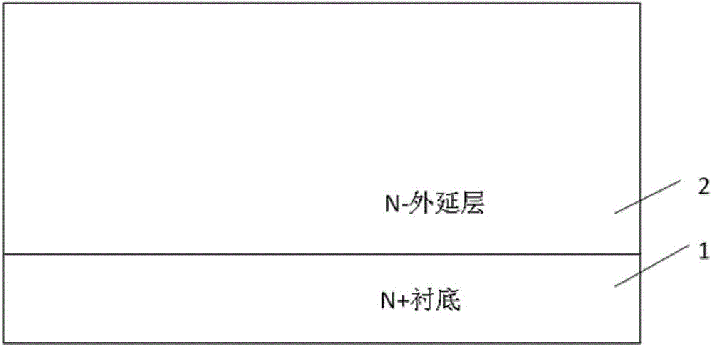
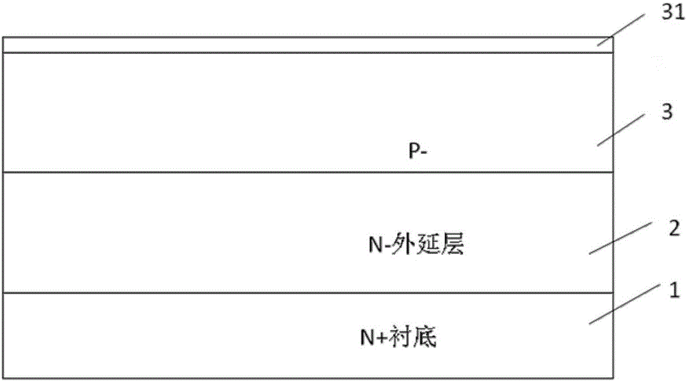
[0031] Such as Figure 12 As shown, a trench-type CoolMOS, from bottom to top includes back metal layer 13, N+ substrate 1, N- epitaxial layer 2, P- well region 3, n+ source region 7, insulating layer 8 and front metal layer 10;

[0032] The N+ substrate 1 is provided with several super junction trenches 11 penetrating through the N+ substrate 1, one end of the super junction trenches 11 extends to the N- epitaxial layer 2, and the inside of the super junction trenches 11 Filled with P-type silicon 12;

[0033] The P-well region 3 is provided with some gate grooves 4 (gate grooves 4 separate the P-well region 3 from each other, and the n+ source region 7 passes through the P-well region 3 and the n+ source region 7). located between the gate trenches 4), one end of the gate trenches 4 extends to the N- epitaxial layer 2, the gate trenches 4 are filled with polysilicon 6, the polysilicon 6 and the gate trenches 4 The vertical distance between the gate trench 4 and the super ...


PUM


Abstract

The invention belongs to the technical field of semiconductor devices, a trench type CoolMOS, which sequentially includes a back metal layer, an N+ substrate, an N epitaxial layer, a P well region, an n+ source region, an insulating layer and a front metal layer from bottom to top; A number of super junction trenches penetrating the N+ substrate are provided on the N+ substrate, one end of the super junction trench extends to the N-epitaxial layer, and the super junction trench is filled with P-type silicon; the P-well region is provided with a penetrating P-well A number of gate trenches in the N+ region and the n+ source region, one end of the gate trench extends to the N-epitaxial layer, the gate trench is filled with polysilicon, and the polysilicon and the gate trench are set by a gate oxide interval; the n+ source region A plurality of contact holes are provided through the n+ source region and the insulating layer, one end of the contact hole extends to the P-well region, the contact holes are filled with conductive metal, and the conductive metal is in contact with the front metal layer. The front adopts a gate trench structure, and the back is dug and filled with P-type silicon to achieve the effect of multiple implantation and diffusion of P-type ions.

Description

technical field [0001] The invention belongs to the technical field of semiconductor devices, in particular to a trench CoolMOS and a manufacturing method thereof. Background technique [0002] Such as figure 1 The traditional CoolMOS structure is shown. CoolMOS is also called super-junction MOS. Due to the adoption of a new withstand voltage layer structure, its electric field distribution is a rectangular structure. Low on-resistance, high voltage resistance, low calorific value. [0003] The super junction structure of CoolMOS is a comb structure, which needs to be formed by multiple ion implantation and secondary high-temperature diffusion, which greatly increases the number of process steps and increases the production cost. Contents of the invention [0004] The purpose of the present invention is to overcome the defects of the complex manufacturing process of CoolMOS in the prior art, and provide a trench-type CoolMOS and its preparation method, which adopts the p...

Claims


Application Information

Patent Timeline
Patent Type & Authority Applications(China)
IPC IPC(8): H01L29/78H01L29/06H01L29/423H01L21/336
CPCH01L29/7828H01L29/0634H01L29/4236H01L29/66666
Inventor 周炳
Owner SUZHOU TONGGUAN MICROELECTRONICS
Learn More