Memory control circuit and memory

A technology for controlling circuits and memory, which is applied in static memory, digital memory information, information storage, etc. It can solve the problems of reduced reading speed, increased local source line voltage, and reduced conduction current of storage cells, so as to improve the reading speed , the effect of increasing the current and reducing the voltage

Active Publication Date: 2019-10-22
SHANGHAI HUAHONG GRACE SEMICON MFG CORP
View PDF5 Cites 0 Cited by
  • Summary
  • Abstract
  • Description
  • Claims
  • Application Information

AI Technical Summary

Problems solved by technology

[0004] However, in the prior art, due to the small size of the word line gating transistor M1 and the source line gating transistor M2, their current conduction capability is weak; during the read operation of the memory, if a single memory cell has a large current, due to the source line selection The conduction ability of the pass tube M2 is weak, the local source line voltage rises, the voltage difference between the drain and source of the memory cell decreases, and the conduction current of the memory cell becomes smaller, resulting in a decrease in the read speed, and the address input to the data output. The required read time (Taa) becomes longer, reducing the efficiency of the memory

Method used


Image

  • Memory control circuit and memory
  • Memory control circuit and memory
  • Memory control circuit and memory

Examples


Embodiment Construction

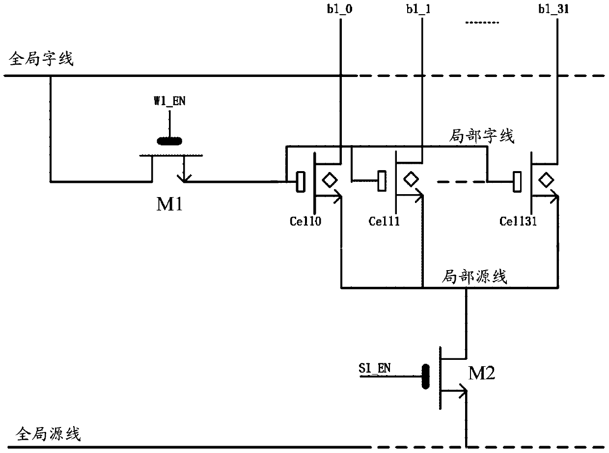
[0023] As mentioned in the background art, in the prior art, due to the small size of the word line gating transistor M1 and the source line gating transistor M2, their current conduction capability is weak; , due to the weak conduction capability of the source line gating tube M2, the local source line voltage rises, the voltage difference between the drain and source of the memory cell decreases, and the conduction current of the memory cell becomes smaller, resulting in a decrease in the read speed and address The read time (Taa) required from input to data output becomes longer, reducing the efficiency of the memory.

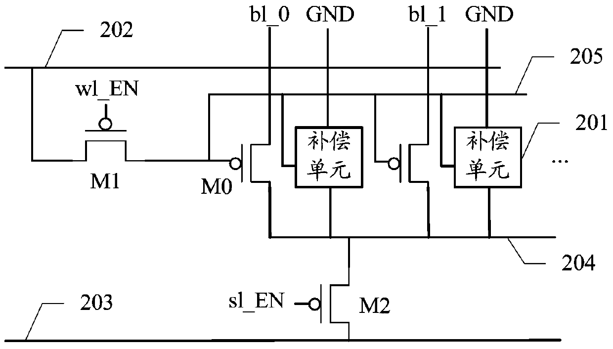
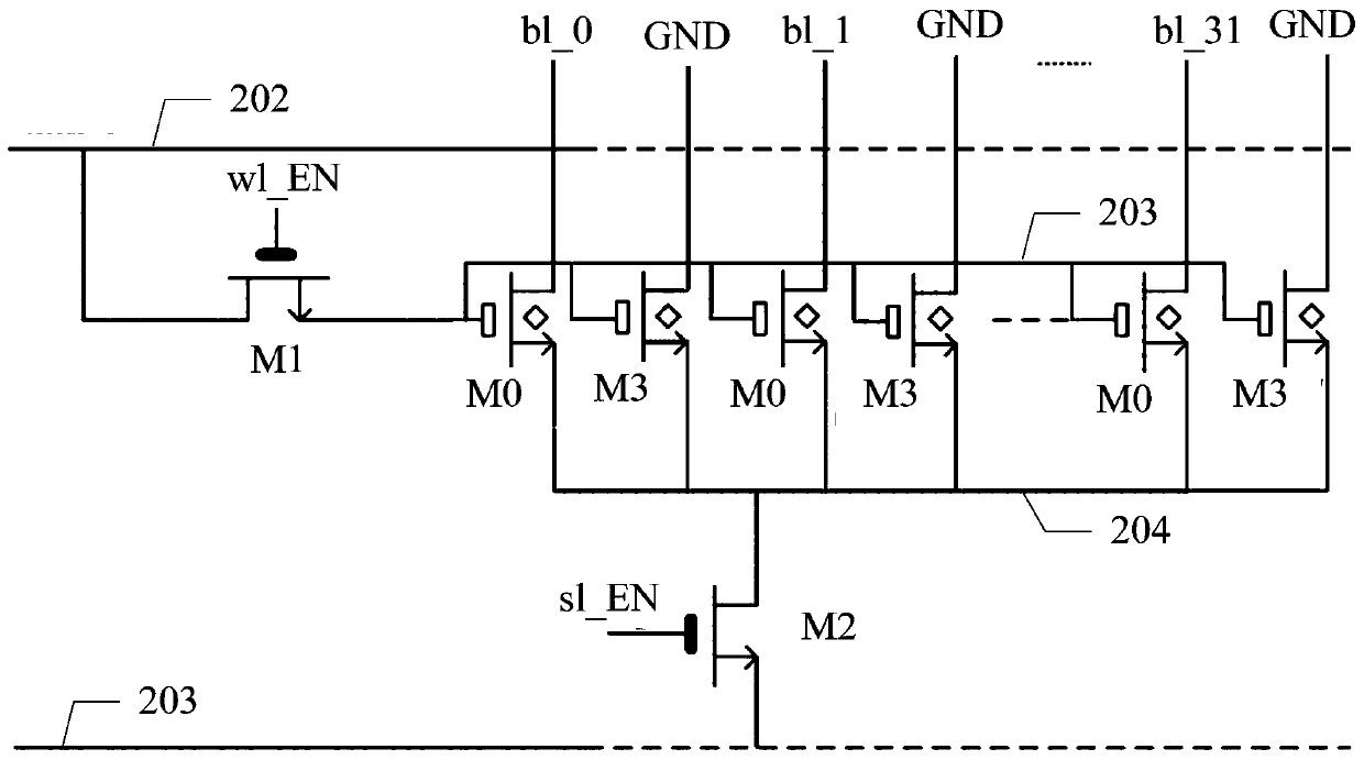
[0024] In order to improve the read speed of the memory, the size of the source line gating transistor M2 can be increased to increase its current conduction capability; however, due to the limitation of the memory chip area, the size increase range of the source line gating transistor M2 is limited. In the embodiment of the present invention, by setting the...


PUM


Abstract

The invention relates to a memory control circuit and a memory. The memory control circuit comprises a source line gate tube and a word line gate tube, the word line gate tube is connected with a memory cell, the source line gate tube is connected with the memory cell through a local source line, the memory control circuit also comprises a compensation unit, and the compensation unit discharges electricity to the local source line in the reading operation in order to reduce the voltage of the local source line. The arrangement of compensation unit reduces the voltage of the local source line in the reading operation and increases a voltage difference between the local word line and the local source line, and the reading time needed from address input to address output becomes short with the increase of the current of the memory cell, so the reading speed of the memory is improved.

Description

technical field [0001] The invention relates to the field of semiconductor integrated circuits, in particular to a memory control circuit and memory. Background technique [0002] With the continuous improvement of semiconductor manufacturing technology and integrated circuit design capabilities, people have been able to integrate processors, memory, analog circuits, interface logic and even radio frequency circuits into one chip, which is the System-on-Chip (System-on-Chip, SoC). With the continuous increase of data throughput and the requirement of low power consumption of the system, the memory requirement of system-on-chip is increasing. It is predicted that about 90% of the silicon chip area will be occupied by memories with different functions in the future, and embedded memories will become the decisive factor dominating the entire system. Represented by flash memory (flash) and Electrically Erasable Programmable Read-Only Memory (EEPROM), non-volatile memory has be...

Claims


Application Information

Patent Timeline
Patent Type & Authority Patents(China)
IPC IPC(8): G11C7/22G11C8/08
Inventor 张勇
Owner SHANGHAI HUAHONG GRACE SEMICON MFG CORP
Why Eureka
Try Eureka