Transistors and methods of forming them

A technology of transistors and semiconductors, applied in semiconductor devices, semiconductor/solid-state device manufacturing, electrical components, etc., can solve the problems of unstable performance of high-k metal gate transistors and increased difficulty in the process of high-k metal gate transistors, achieving performance improvement, Good shape and stable threshold voltage

Active Publication Date: 2019-01-29
SEMICON MFG INT (SHANGHAI) CORP
View PDF5 Cites 0 Cited by
  • Summary
  • Abstract
  • Description
  • Claims
  • Application Information

AI Technical Summary

Problems solved by technology

[0005] However, with the continuous shrinking of semiconductor process nodes, the size of the formed high-K metal gate transistors is continuously reduced, which leads to an increase in the process difficulty of manufacturing high-K metal gate transistors, and the performance of the formed high-K metal gate transistors is unstable.

Method used


Image

  • Transistors and methods of forming them
  • Transistors and methods of forming them
  • Transistors and methods of forming them

Examples


Embodiment Construction

[0035] As mentioned in the background art, with the continuous reduction of semiconductor process nodes, the size of the formed high-k metal gate transistors is continuously reduced, which leads to an increase in the process difficulty of manufacturing high-k metal gate transistors, and the formed high-k metal gate transistors Performance is unstable.

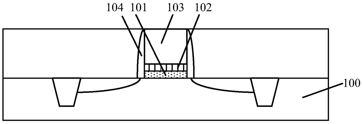
[0036] Please refer to figure 1 , figure 1A schematic cross-sectional structure diagram of a high-K metal gate transistor according to an embodiment of the present invention, comprising: a substrate 100; a gate structure located on the surface of the substrate 100, the gate structure comprising: a high-K gate dielectric layer located on the surface of the substrate 101; the capping layer 102 on the surface of the high-K gate dielectric layer 101; the metal gate 103 on the surface of the capping layer 102; the sidewalls 104 on the sidewall surfaces of the metal gate 103, the capping layer 102 and the high-K gate dielectric laye...


PUM


Abstract

The invention relates to a transistor and a formation method thereof. The formation method of the transistor comprises the steps of providing a substrate, forming a gate structure at the surface of the substrate, wherein the gate structure comprises a gate dielectric layer, a protection layer located at the surface of the gate dielectric layer and a gate layer located at the surface of the protection layer, forming a first side wall at the side wall surface of the gate structure, etching the substrate around the gate structure and the first side wall by adopting an over etching process so as to enabling the surface of the substrate to be lower than the bottom surface of the gate structure, and forming a second side wall at the surface of the first side wall after the first over etching process. The formed transistor is improved in shape and stable in performance.

Description

technical field [0001] The invention relates to the technical field of semiconductor manufacturing, in particular to a transistor and a forming method thereof. Background technique [0002] With the rapid development of integrated circuit manufacturing technology, the size of semiconductor devices in integrated circuits, especially MOS (Metal Oxide Semiconductor, metal-oxide-semiconductor) devices, is continuously reduced to meet the miniaturization and development of integrated circuits. Integration requirements, and transistor devices are one of the important components of MOS devices. [0003] For transistor devices, as the size of the transistor continues to shrink, the gate dielectric layer formed of silicon oxide or silicon oxynitride material in the prior art cannot meet the performance requirements of the transistor. In particular, transistors formed with silicon oxide or silicon oxynitride as the gate dielectric layer are prone to a series of problems such as leaka...

Claims


Application Information

Patent Timeline
Patent Type & Authority Patents(China)
IPC IPC(8): H01L29/423H01L21/336
Inventor 邓浩徐建华
Owner SEMICON MFG INT (SHANGHAI) CORP
Why Eureka
Try Eureka