
Parallel and WDM silicon photonics integration in information and communications technology systems

A signal, silicon waveguide technology, applied in the field of information and communication technology systems, which can solve the problems of high cost and high power consumption

Active Publication Date: 2016-07-27
TELEFON AB LM ERICSSON (PUBL)
View PDF5 Cites 14 Cited by
  • Summary
  • Abstract
  • Description
  • Claims
  • Application Information

AI Technical Summary

Problems solved by technology

Although this operation can be achieved by using different optical transceiver modules via O-E-O (optical-electrical-optical) two-stage conversion, this process is very expensive, and the power consumption on the electronics alone is very high, especially for High bit rates where CDR (Clock Data Recovery) as well as signal processing and regeneration are necessary

Method used


Image

  • Parallel and WDM silicon photonics integration in information and communications technology systems
  • Parallel and WDM silicon photonics integration in information and communications technology systems
  • Parallel and WDM silicon photonics integration in information and communications technology systems

Examples


Embodiment Construction

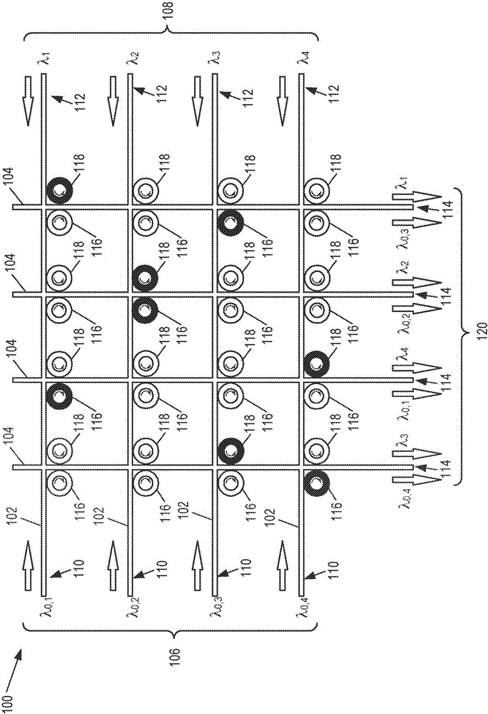
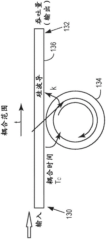
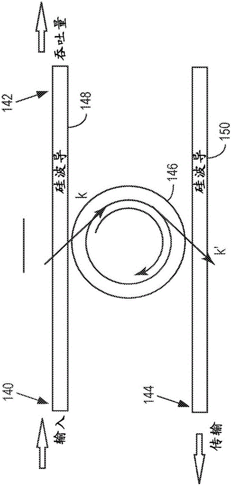
[0023] An all-optical wavelength converter is provided. The wavelength converter includes intersecting silicon waveguides making up the arrayed waveguide and microring resonators forming the arrayed waveguide, and a nonlinear medium coupled to the output of the arrayed waveguide. Gray light (ie single wavelength) is converted into a wavelength division multiplexed (WDM) optical signal by an all-optical wavelength converter. By providing all-optical conversion that is wavelength, polarization, and data format transparent, the all-optical wavelength converter eliminates the need for two-stage OEO and does not require additional electrical signal processing. Microring resonators included in the arrayed waveguides are used as routing and switching elements to rearrange and combine the entrance gray light parallel data signal lines with selected optical pump signals. Microring resonators consume very little power and can provide variable tuning, enabling networking features that c...


PUM


Abstract

A wavelength converter includes first silicon waveguides (102) and second silicon waveguides (104) intersecting the first silicon waveguides (102) to form an arrayed waveguide (100). The arrayed waveguide (100) receives optical data signals at the same wavelength at a first input (106) and optical pump signals at different wavelengths at a second input (108). Microring resonators (114, 116) evanescently couple different ones of the first silicon waveguides (102) to different ones of the second silicon waveguides (104). Each microring resonator (114, 116) is tuned to the wavelength of the optical data signals or one of the wavelengths of the optical pump signals, so that different combinations of the optical data signals and the optical pump signals are provided at an output (120) of the arrayed waveguide (100). A non-linear optical media (200) converts the wavelength of each combined optical signal at the output (120) of the arrayed waveguide (100) to yield wavelength converted signals each having a new dedicated wavelength.

Description

technical field [0001] The present invention relates generally to information and communication technology systems, and more particularly to parallel and WDM photonic integration for information and communication technology systems. Background technique [0002] In large-scale information and communication technology (ICT) systems (such as data center networks), optical interconnects, especially silicon photonics, are enabling Mature CMOS (complementary metal oxide semiconductor) technology (processes) compatible, monolithic integration and other advantages of technology become possible. For very short-reach applications such as chip-to-chip, block-to-block, and line-card-to-line card interconnects, gray-light (ie, single-wavelength) parallel silicon photonics is very cost-effective. Gray-light parallel silicon photonics can extend the range to thousands of meters. WDM (Wavelength Division Multiplexing) silicon photonic modules using multi-wavelength laser arrays at the tr...

Claims


Application Information

Patent Timeline
IPC IPC(8): G02F2/00G02B6/12H04J14/02
CPCG02B6/12007G02F1/353G02F1/365G02F2/004G02F2/006H04Q11/0005H04Q2011/0011H04Q2011/0035H04J14/0212
Inventor 徐清R·布伦纳S·莱萨德
Owner TELEFON AB LM ERICSSON (PUBL)
Learn More