Thick film chip resistor structure

A chip resistor, thick film technology, applied in the direction of electric solid devices, circuits, electrical components, etc., can solve the problems of increasing processing difficulty, increasing production costs, and low economic benefits, improving heat dissipation effect and overall power, and increasing overall heat dissipation. The effect of volume and high economic efficiency

Inactive Publication Date: 2016-07-20
ROYAL ELECTRONICS FTY
View PDF4 Cites 0 Cited by
  • Summary
  • Abstract
  • Description
  • Claims
  • Application Information

AI Technical Summary

Problems solved by technology

[0004] The resistance value of the chip resistor can be directly represented by the three-digit code on the appearance of the chip resistor body, and the resistance value of the chip resistor is mainly obtained by printing a resistance layer on the surface of the ceramic substrate to obtain a rough initial value of the resistance value. Subsequent laser trimming is necessary to obtain the required precise resistance value. The method of resistor laser trimming is mainly to trim the surface of the chip resistor, and adjust the resistance value by reducing the cross-sectional area of ​​the chip resistor. Generally, the laser cutting method on the surface of the resistor is to cut an L-shaped incision 11 on the surface of the resistor 10 to adjust the resistance value. However, the L-shaped incision 11 is to destroy the resistance layer in a large area at one time. Accurately grasping the machining accuracy will result in inaccurate resistance values. Of course, obtaining precise resistance values ​​will greatly increase the difficulty of processing and increase production costs at the same time, but there is a lack of economic benefits.

Method used


Image

  • Thick film chip resistor structure
  • Thick film chip resistor structure
  • Thick film chip resistor structure

Examples


Embodiment Construction

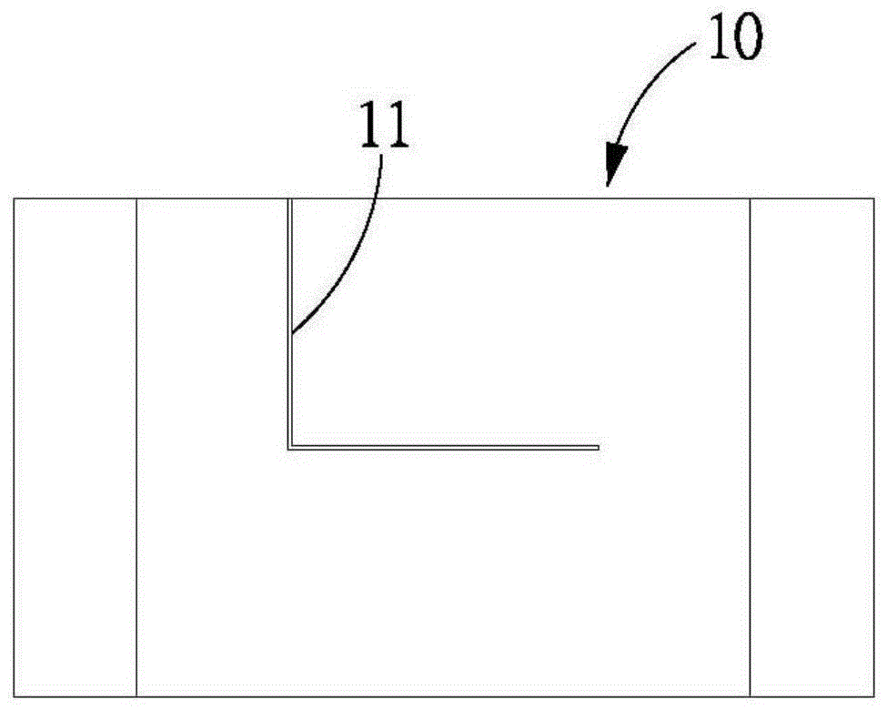
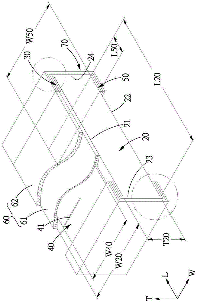
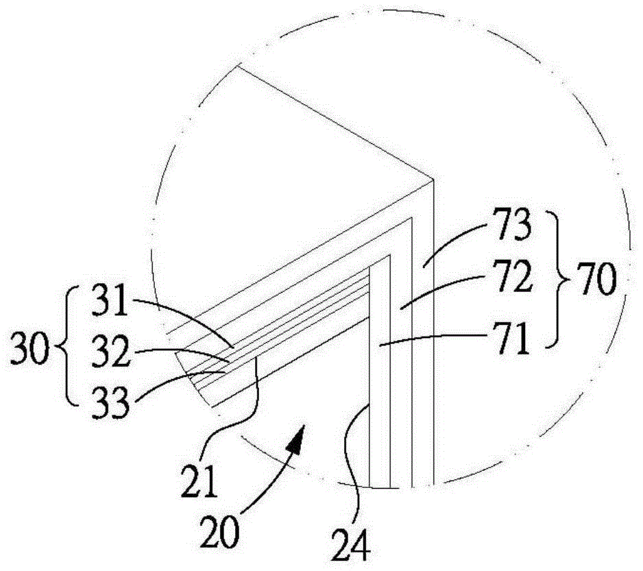
[0037] A preferred embodiment of the thick film chip resistor structure of the present invention is shown in Figures 2 to 3,

[0038] The thick film chip resistor structure of the present invention comprises:

[0039] A substrate 20 is made of high-purity alumina porcelain, and the substrate 20 is a square block structure formed along the length direction L, width direction W, and thickness direction T, wherein the length direction L, width direction W and the The thickness direction T is a three-dimensional direction perpendicular to each other, the substrate 20 has a length dimension L20 in the length direction L, the substrate 20 has a width dimension W20 in the width direction W, and the substrate 20 has a thickness dimension in the thickness direction T T20, the length dimension L20 is 6.35 millimeters, the width dimension W20 is 3.20 millimeters, and the thickness dimension T20 is 1 millimeter; and the two ends of the substrate 20 in the thickness direction T are respect...


PUM


Abstract

The invention discloses a thick film chip resistor structure. The heat dissipation volume of an overall resistor is effectively improved under the premise of maintaining an idiomatic 2512 chip resistor by increasing the thickness dimension of a substrate, increasing the layer number of composition of an upper electrode unit, increasing the layer number of composition of a protection unit and expanding the area of a lower electrode unit and the area of a resistive layer, so that the overall power is significantly improved; the thick film chip resistor structure can provide relatively high power in the same dimension; the applicability is improved; and relatively high economic benefits can be created.

Description

technical field [0001] The present invention relates to the structure of thick film chip resistors, which is related to the structure of the resistors. Background technique [0002] The chip resistors of passive components can be divided into thick-film resistors and thin-film resistors according to different manufacturing processes. Thin-film resistors are made of resistive films by sputtering. Resistors are printed and sintered to make resistive films; the main difference between thick film resistors and thin film resistors lies in the tolerance of precision errors, and users choose different resistors according to product requirements. [0003] In addition to the difference in precision, chip resistors also have differences in size specifications. Common resistor codes are represented by four digits, such as 0402, 0606, 0805 or 2512, which represent the length and width of the resistor. , the first two digits are the length (inches) of the resistor, and the last two digi...

Claims


Application Information

Patent Timeline
Patent Type & Authority Applications(China)
IPC IPC(8): H01L23/64
Inventor 林成信周金源王建国
Owner ROYAL ELECTRONICS FTY
Why Eureka
Try Eureka