
SRAM memory cell and circuit for improving read/write stability of SRAM memory cell

A storage unit and stable technology, applied in the direction of information storage, static memory, digital memory information, etc., can solve the problems of increasing the complexity of the circuit, increasing the memory area, etc., to save area, improve reliability, and good read and write ability Effect

Active Publication Date: 2016-06-01
SPREADTRUM COMM (SHANGHAI) CO LTD
View PDF3 Cites 4 Cited by
  • Summary
  • Abstract
  • Description
  • Claims
  • Application Information

AI Technical Summary

Problems solved by technology

This increases the complexity of the circuit to a certain extent, and the additional auxiliary circuit will also increase the area of ​​the entire memory

Method used


Image

  • SRAM memory cell and circuit for improving read/write stability of SRAM memory cell
  • SRAM memory cell and circuit for improving read/write stability of SRAM memory cell
  • SRAM memory cell and circuit for improving read/write stability of SRAM memory cell

Examples


specific Embodiment

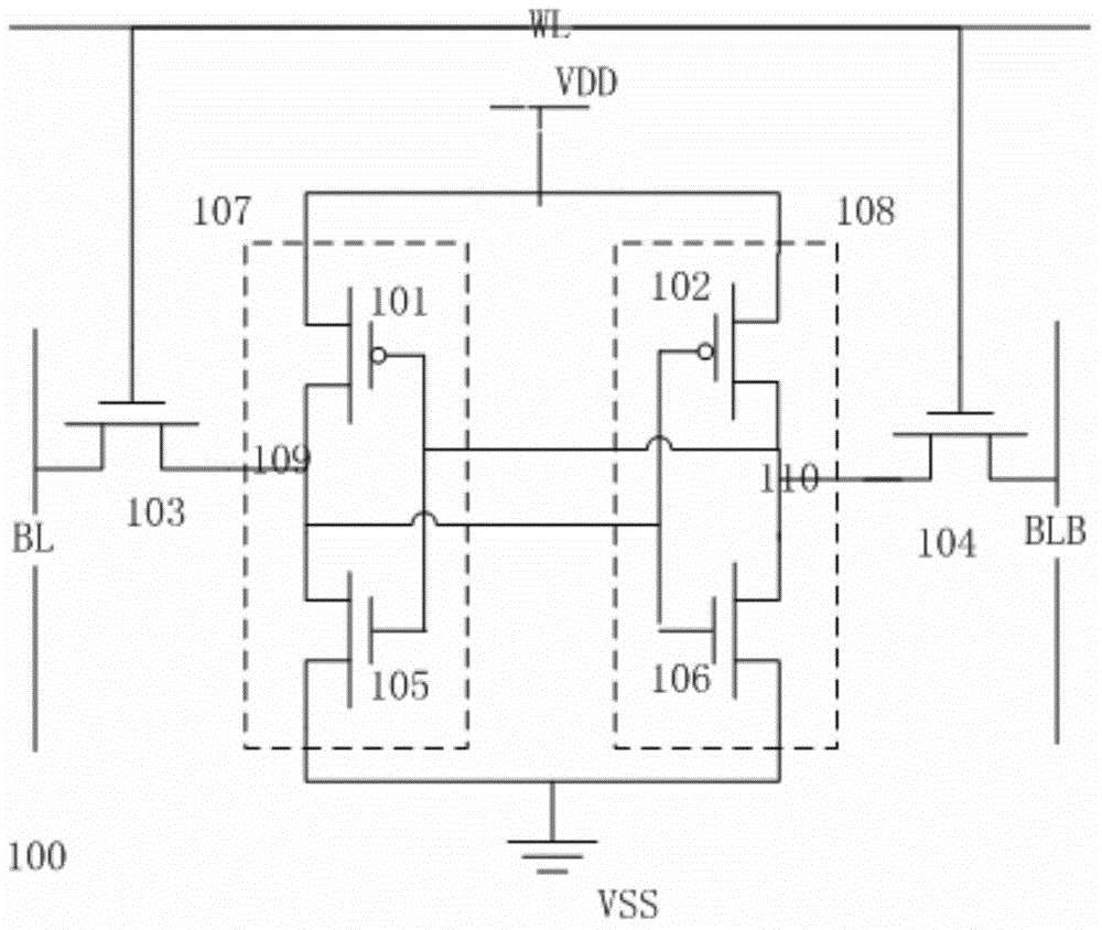
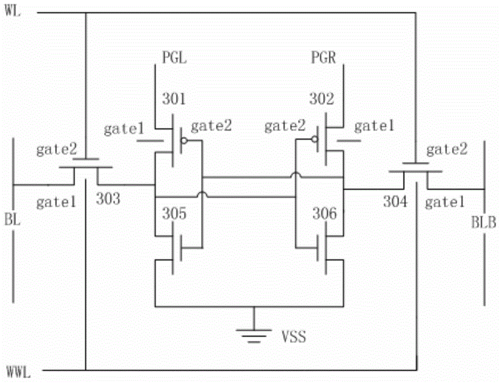
[0068] In a specific embodiment, the first PMOS transistor 301 and the second PMOS transistor 302 adopt independent gate mode FINFET devices; the first NMOS transistor 305 and the second NMOS transistor 306 adopt common gate mode FINFET devices. The first switching device 303 and the second switching device 304 adopt NMOS transistors, independent gate mode FINFET devices; the first grid gate1 is connected to the write word line WWL, and the second grid gate2 is connected to the word line WL; the first PMOS transistor 301 Both the first grid gate1 and the second PMOS transistor 302 are connected to the power supply voltage VDD, so that the first grid gate1 is in an off state, and the first PMOS transistor 301 and the second PMOS transistor are controlled by the second grid gate2 The turn-on and turn-off of 302, compared with the device whose channel is jointly controlled by the first gate gate1 and the second gate gate2, has a weakened drive capability, which can improve the wri...


PUM


Abstract

The invention relates to the technical field of electronic communication, in particular to an SRAM memory cell and a circuit for improving the read / write stability of the SRAM memory cell. The SRAM memory cell comprises a first switch device, a second switch device, a first inverse unit and a second inverse unit, wherein the first switch device is controllably connected with a first bit line to a first memory code; the second switch device is controllably connected with a second bit line to a second memory code; the first inverse unit is connected between the first switch device and the second switch device in series; the first inverse unit is provided with a first input end and a first output end; the first memory code is defined at the first output end; the second inverse unit is connected between the first switch device and the second switch device in series; a second input end of the second inverse unit is connected with the first output end; a second output end of the second inverse unit is connected with the first input end; and the second memory code is defined at the second output end. According to the SRAM memory cell and the circuit, better read / write ability is provided, the reliability of the SRAM memory cell is improved without adding overmuch extra circuits, the complexity of circuit design is reduced and the area is saved.

Description

technical field [0001] The invention relates to the technical field of electronic communication, in particular to an SRAM storage unit and a circuit for improving its reading and writing stability. Background technique [0002] SRAM (Static RAM, static random access memory) memory is a memory with static access function. It can save the data stored in it without refreshing the circuit. It plays an important role in each chip system. For a SRAM storage unit , its stability is crucial. A storage unit with strong writing ability can not only ensure the stability of the unit, but also increase the speed of writing operations, so that the entire memory can work in a higher-speed system, so its performance also determines the performance of the entire chip. . [0003] With the continuous advancement of the advanced technology level, the size of the device is getting smaller and smaller, and the drift deviation of the process parameters is inevitable, especially for the SRAM arra...

Claims


Application Information

Patent Timeline
IPC IPC(8): G11C11/413G11C11/419
Inventor 吴守道郑坚斌于跃王林黄瑞锋
Owner SPREADTRUM COMM (SHANGHAI) CO LTD
Learn More