Probe for scanning probe microscope, preparation method of the probe, and detection method of the probe
A scanning probe and microscope technology, applied in the probe field of scanning probe microscope, can solve problems such as limiting in-depth understanding of research, obtaining single thermal information, coupled imaging, etc.
- Summary
- Abstract
- Description
- Claims
- Application Information
AI Technical Summary
Problems solved by technology
Method used
Image
Examples
Embodiment 1
[0123] In this embodiment, the scanning probe microscope includes a scanning probe microscope platform, a probe, an electrical signal application unit, a displacement or vibration signal acquisition unit, a thermal signal acquisition unit, an electrical signal acquisition unit, and a central control unit. The probe control unit is used to drive or control the probe to move and / or vibrate. Central control unit: used to initialize each unit of the system, control each unit of the system, receive the shape, heat, and electrical signals of the sample, and obtain the image of the shape, heat, and electrical signals of the sample after analysis;
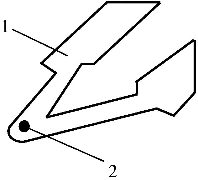
[0124] Such as figure 1As shown, the probe includes a probe arm 1 and a needle tip 2 .
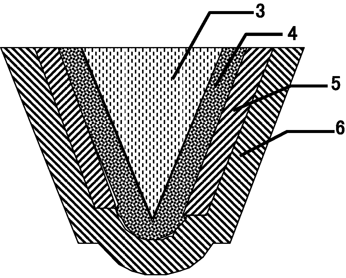
[0125] The structure of needle tip 2 is as follows figure 2 As shown, it is composed of the needle tip body 3 and the surface covering layer. The surface covering layer is composed of film one 4 , film one 4 covering the surface of film two 5 , and ...
Embodiment 2
[0149] In this embodiment, the structure of the scanning probe microscope is exactly the same as that in Embodiment 1.
[0150] The difference is that the probe tip with a thermocouple structure is prepared by another method, which includes the following steps:
[0151] Step 1. Using the coating method, film one 4, film two 5 and film three 6 are sequentially prepared on the surface of the needle tip body 3;
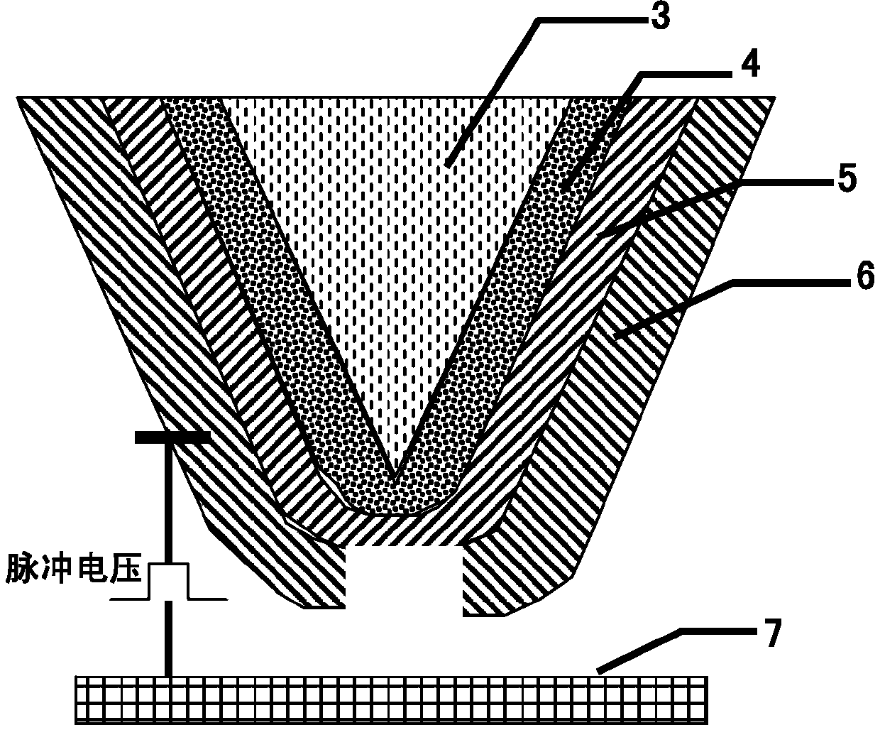
[0152] Step 2. Apply a voltage between the film 3 6 and the electrode layer 7, and use the tip discharge principle to adjust the distance between the film 3 6 and the electrode layer 7 to melt the film 3 6 at the tip of the needle point, exposing the film 2 5, and Other parts of the film 36 are not melted;
[0153] Step 3: remove the exposed film 2 5 described in step 2, and expose the film 1 4;
[0154] Step 4: Coating the exposed part with the same material as thin film three 6, so that thin film one 4 and thin film three 6 are connected at the tip of the needle tip ...
Embodiment 3
[0157] In this embodiment, the structure of the scanning probe microscope is basically the same as that in Embodiment 1, except that a probe with a thermal resistance structure is used.
[0158] Such as figure 1 As shown, the probe includes a probe arm 1 and a needle tip 2 . Tip 2 as Figure 4 As shown, it includes a needle point body 3, a thermal resistance material layer 8, a first conductive layer 9 and a second conductive layer 10; the thermal resistance material layer 8 is located on the surface of the needle point body 3, and the second conductive layer 10 is located on the surface of the thermal resistance material layer; A conductive layer 9 is in electrical communication with the thermal resistance material layer 8 .
[0159] The thermal resistance material layer 8 is made of low-doped silicon with a thickness of 2m, and the conductive layer 9 is made of bismuth (Bi), nickel (Ni), cobalt (Co), potassium (K), graphite, and graphene. , the thickness is 1 μm, the mate...
PUM
 Abstract
Description
Claims
Application Information
 - Generate Ideas
- Intellectual Property
- Life Sciences
- Materials
- Tech Scout
- Unparalleled Data Quality
- Higher Quality Content
- 60% Fewer Hallucinations
Browse by: Latest US Patents, China's latest patents, Technical Efficacy Thesaurus, Application Domain, Technology Topic, Popular Technical Reports.
© 2025 PatSnap. All rights reserved.Legal|Privacy policy|Modern Slavery Act Transparency Statement|Sitemap|About US| Contact US: help@patsnap.com


