Method for producing package substrate

A technology for encapsulating substrates and manufacturing methods, applied in semiconductor/solid-state device manufacturing, electrical components, circuits, etc., can solve problems such as the Giavani effect and achieve the effect of protecting the metallization layer

Active Publication Date: 2016-04-13
SHENNAN CIRCUITS
View PDF3 Cites 5 Cited by
  • Summary
  • Abstract
  • Description
  • Claims
  • Application Information

AI Technical Summary

Problems solved by technology

[0006] An embodiment of the present invention provides a method for manufacturing a packaging substrate, which is used to solve the problem of Giavani effect in the prior art

Method used


Image

  • Method for producing package substrate
  • Method for producing package substrate
  • Method for producing package substrate

Examples


Embodiment 1

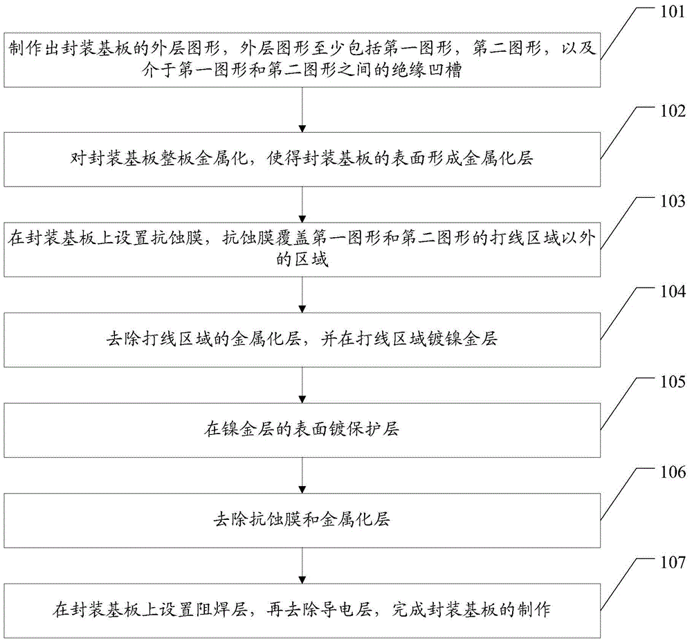
[0024] Please refer to figure 1 , an embodiment of the present invention provides a method for manufacturing a packaging substrate, which may include:

[0025] 101. Fabricate the outer pattern of the packaging substrate, the outer pattern at least includes a first pattern, a second pattern, and an insulating groove between the first pattern and the second pattern;

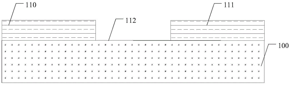
[0026] Please refer to figure 2 , making the outer pattern of the packaging substrate, the outer pattern is attached to the substrate 100, the outer pattern at least includes a first pattern 110, a second pattern 111, and a pattern between the first pattern 110 and the second pattern 111 The insulating groove 112 between them.

[0027] It should be noted that the substrate may be a substrate composed of resin glass fibers, which is not specifically limited here.

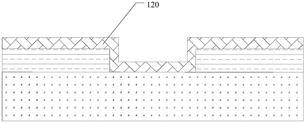
[0028] 102. Metallize the entire package substrate, so that a metallized layer is formed on the surface of the package substrate;

[0029] Please re...


PUM


Abstract

The invention discloses a method for producing a package substrate. The method includes the following steps of: producing an outer graph, wherein the outer graph at least includes a first graph, a second graph, and an insulation groove arranged between the first graph and the second graph; performing metallization on the whole package substrate to allow a surface of the package substrate to form a metallization layer; arranging a corrosion-resistant film which covers areas of the first graph and the second graph except line areas; removing the metallization layer on the line areas, and plating a nickel gold layer onto the line areas; plating a protective layer onto a surface of the nickel gold layer; removing the corrosion-resistant film and the metallization layer; arranging a solder resist layer on the package substrate, and removing the protective layer to complete production of the package substrate. The method can be used to solve the problem in the prior art of galvanic effect.

Description

technical field [0001] The invention relates to the technical field of circuit boards, in particular to a method for manufacturing a packaging substrate. Background technique [0002] With the continuous development of electronic products in the direction of miniaturization, thinning and multi-function, integrated circuit packaging is also required to develop in the direction of thinning and high density. As the carrier of integrated circuit packaging, the wiring density of the packaging substrate is also increasing. keep improving. [0003] At present, many integrated circuit packages adopt the wire bonding process, which requires the substrate bonding fingers to be treated with electroplated nickel gold. Due to the increase in wiring density, many substrates have no space for separate design of electric gold leads. Therefore, it is necessary to use leadless electro-gold technology. The lead electro-gold process is usually electroplated nickel-gold on the wire-bonding fing...

Claims


Application Information

Patent Timeline
Patent Type & Authority Applications(China)
IPC IPC(8): H01L21/48
Inventor 谷新
Owner SHENNAN CIRCUITS
Why Eureka
Try Eureka