
Surface plasmon waveguide

A surface plasmon and waveguide technology, applied in the field of waveguides, can solve the problems of limited turning radius, crosstalk, turning angle limitation, etc.

Inactive Publication Date: 2016-02-17
BEIJING SAMSUNG TELECOM R&D CENT +2
View PDF0 Cites 14 Cited by
  • Summary
  • Abstract
  • Description
  • Claims
  • Application Information

AI Technical Summary

Problems solved by technology

Because the surface plasmons at the interface between the core layer and the cladding layer propagate along the waveguide in the form of total internal reflection, resulting in a certain proportion of energy propagation in the cladding layer, making the energy localization worse
In addition, in the above two waveguide structures, if the distance between the two waveguides is relatively close, there will be overlap of modes and crosstalk. At the same time, the above two waveguides have restrictions on the turning radius when turning, and the turning with a small turning radius cannot be realized. The turning radius is not too large. For example, if the turning radius does not exceed the equivalent wavelength, there are also restrictions on the turning angle, and it is impossible to achieve a large-angle turn of 180 degrees or even 360 degrees.

Method used


Image

  • Surface plasmon waveguide
  • Surface plasmon waveguide
  • Surface plasmon waveguide

Examples


Embodiment Construction

[0044] In order to make the purpose, technical solution and advantages of the present invention more clear, the present invention will be further described in detail below with reference to the accompanying drawings and examples.

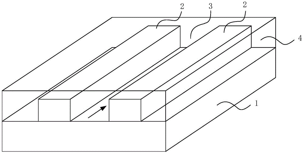
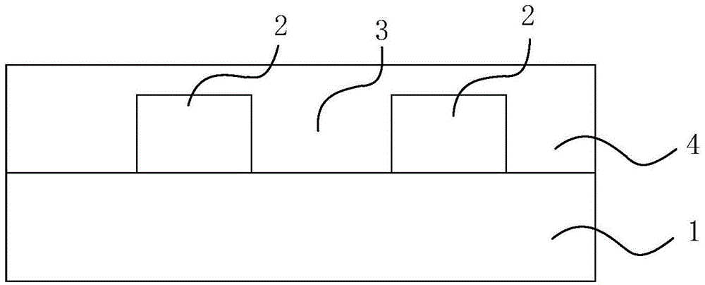
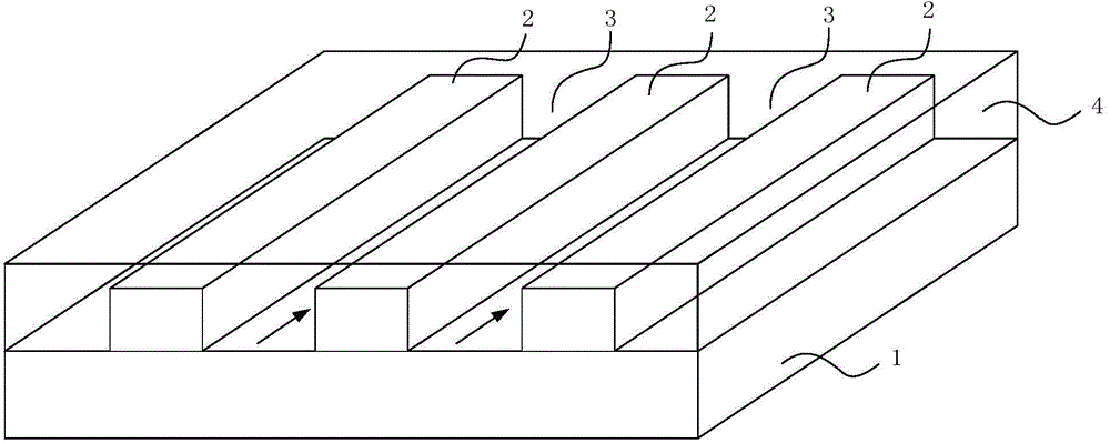
[0045] The surface plasmon waveguide of the present invention mainly includes a metal substrate and at least two metal walls located on the substrate and parallel to each other; wherein, a groove is formed between the metal walls, and a groove is formed between the grooves. Inside, due to the constraint of the metal wall to form a lateral localized electromagnetic field from metal wall to metal wall, surface plasmons propagate on the surface of the metal substrate at the bottom of the trench along the extending direction of the trench.

[0046] Figure 1a It is a schematic structural diagram of a specific embodiment of the surface plasmon waveguide of the present invention, Figure 1b for Figure 1a A cross-sectional view of the structure of the ill...


PUM

PropertyMeasurementUnit
Heightaaaaaaaaaa
Thicknessaaaaaaaaaa

Abstract

Disclosed in the invention is a surface plasmon waveguide comprising a metal substrate and at least two metal walls. The at least two metal walls arranged on the substrate are parallel to each other. A groove is formed between the metal walls, so that the surface plasmon can be transmitted at the metal substrate surface at the bottom of the groove along the extending direction of the groove. According to the invention, because of the metal walls at the surface of the metal substrate, an electromagnetic filed with transverse locality can be formed in the groove between the metal walls from the metal wall to the metal wall, thereby limiting transmission of the surface plasmon to the outside of the metal walls. Therefore, the surface plasmon only can be transmitted along the interfaces of the metal substrate and the dielectric layer between the two metal walls at the direction parallel to the metal walls. Because the metal walls play a good role in limiting the surface plasmon in the waveguides, the crosstalk between waveguides can be avoided even though the interval between the two waveguides is small. With the surface plasmon waveguide, small-radius large-angle turning transmission of the surface plasmon as well as application to an optical beam splitter can be realized.

Description

technical field [0001] The invention relates to the field of waveguides, in particular to a surface plasmon waveguide. Background technique [0002] When a light wave (electromagnetic wave) is incident on the interface between the metal and the medium, the free electrons on the metal surface will oscillate collectively, and the light wave is coupled with the free electrons near the metal surface to form a near-field electromagnetic wave that propagates along the metal surface. If the oscillation frequency of the free electrons on the metal surface is consistent with the frequency of the incident light wave, resonance will occur. In the resonance state, the energy of the electromagnetic field is effectively converted into the collective vibration energy of the free electrons on the metal surface. At this time, a A special electromagnetic mode: the electromagnetic field is localized and strengthened within a small area of ​​the metal surface. This phenomenon is called surface...

Claims


Application Information

Patent Timeline
IPC IPC(8): G02B6/122
Inventor 张家森胡闯徐亮金勇朴硏相
Owner BEIJING SAMSUNG TELECOM R&D CENT
Learn More