


Quick Research
Generate reliable direction feasibility study reports for your R&D in just a few steps.

Technical Q&A
Discover and master advanced knowledge NOW. Basics, ideas, possibilities, all at once.

Find Solutions
As an expert in R&D theories, this can generate solutions to your technical problems instantly.

Evaluate Feasibility
Analyze your overall solution with one click, know your potential R&D risks in advance.

Monitor Landscape
Get weekly tech updates, stay abreast of the latest tech innovations and key insights.
Substrate for electronic device package, electronic device package, electronic device, and method of manufacturing electronic device
A technology for electronic devices and manufacturing methods, which is applied in the manufacture of semiconductor/solid-state devices, electric solid-state devices, and components of semiconductor/solid-state devices, etc., can solve the problem of decreased airtightness of storage space, insufficient bonding of lids, and difficult shape of mother substrates. /size etc.
- Summary
- Abstract
- Description
- Claims
- Application Information
AI Technical Summary
Problems solved by technology
Method used
Image

Examples
no. 1 Embodiment approach >
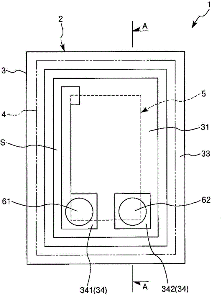
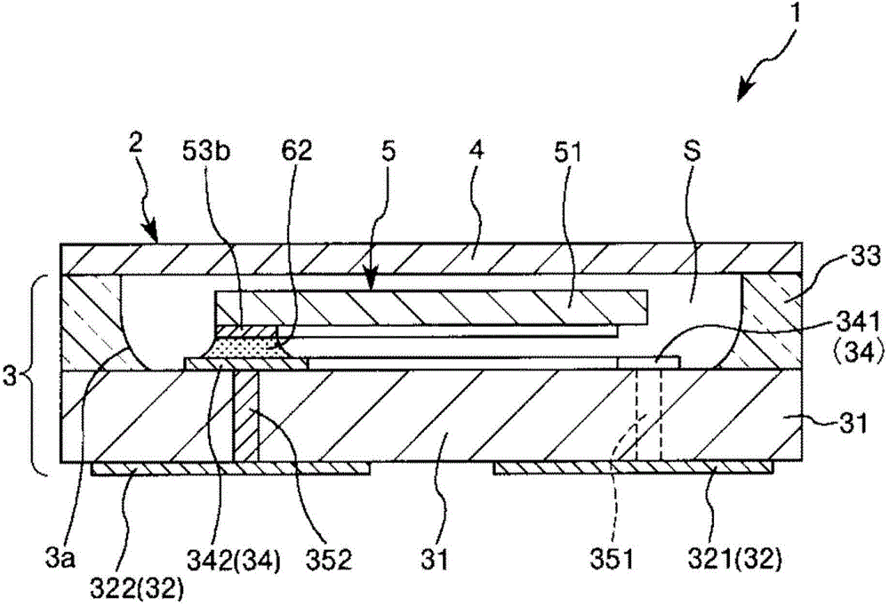
[0067] figure 1 It is a plan view showing the electronic device according to the first embodiment of the present invention. figure 2 Yes figure 1 The A-A line sectional view in. image 3 is showing figure 1 The shown electronic device has a top view of the vibrating element. Figure 4 is to show the figure 1 This is a cross-sectional view showing a state in which an electronic component is mounted on a circuit board. Figure 5 ~ Figure 8 are used to illustrate figure 1 A cross-sectional view of the fabrication method of the electronic device is shown. Also, in the following description, the figure 1 The near front side of the paper in and figure 2 The upper side in is called "upper", and the figure 1 inside of the paper in and figure 2 The lower side in is referred to as "lower".
[0068] "Electronic Devices"
[0069] like figure 1 and figure 2 As shown, an electronic device 1 serving as a vibrator has a package (electronic device package) 2 and a vibrating e...
no. 2 Embodiment approach >
[0108] Figure 9 It is a sectional view showing the electronic device according to the second embodiment of the present invention. Figure 10 is for illustration Figure 9 A cross-sectional view of a method of manufacturing a base substrate of an electronic device is shown.
[0109] Hereinafter, the electronic device according to the second embodiment of the present invention will be described, focusing on the differences from the above-mentioned embodiment, and the description of the same matters will be omitted.
[0110] The electronic device of the second embodiment is the same as that of the above-mentioned first embodiment except that the structure of the package is different. In addition, the same code|symbol is attached|subjected to the same structure as the above-mentioned embodiment.
[0111] like Figure 9As shown, in the base substrate 3 of the present embodiment, a pair of convex portions 391 and 392 protruding from the bottom surface of the concave portion 3 a...
no. 3 Embodiment approach >
[0118] Figure 11 It is a cross-sectional view showing an electronic device according to a third embodiment of the present invention.
[0119] Hereinafter, the electronic device according to the third embodiment of the present invention will be described, focusing on the differences from the above-mentioned embodiment, and the description of the same matters will be omitted.
[0120] The electronic device of the third embodiment is the same as that of the above-mentioned first embodiment except that the structure of the base substrate is different. In addition, the same code|symbol is attached|subjected to the same structure as the above-mentioned embodiment.
[0121] like Figure 11 As shown, in the base substrate 3 of the present embodiment, the first layer 31 is constituted by a laminate in which two ceramic layers 31A, 31B are laminated. Furthermore, an internal wiring layer 38 having a wiring 381 connecting the internal connection terminal 341 and the external connecti...
PUM
 Abstract
Description
Claims
Application Information
 - R&D Engineer
- R&D Manager
- IP Professional
- Industry Leading Data Capabilities
- Powerful AI technology
- Patent DNA Extraction
Browse by: Latest US Patents, China's latest patents, Technical Efficacy Thesaurus, Application Domain, Technology Topic, Popular Technical Reports.
© 2024 PatSnap. All rights reserved.Legal|Privacy policy|Modern Slavery Act Transparency Statement|Sitemap|About US| Contact US: help@patsnap.com