A Gaas-based room temperature infrared luminescent material based on bismuth element and its preparation method
A technology of infrared luminescence and elements, which is applied in the direction of luminescent materials, chemical instruments and methods, lasers, etc., can solve the problem that the luminous wavelength of semiconductor materials is difficult to expand the communication window and other problems
- Summary
- Abstract
- Description
- Claims
- Application Information
AI Technical Summary
Problems solved by technology
Method used
Image
Examples
Embodiment 1
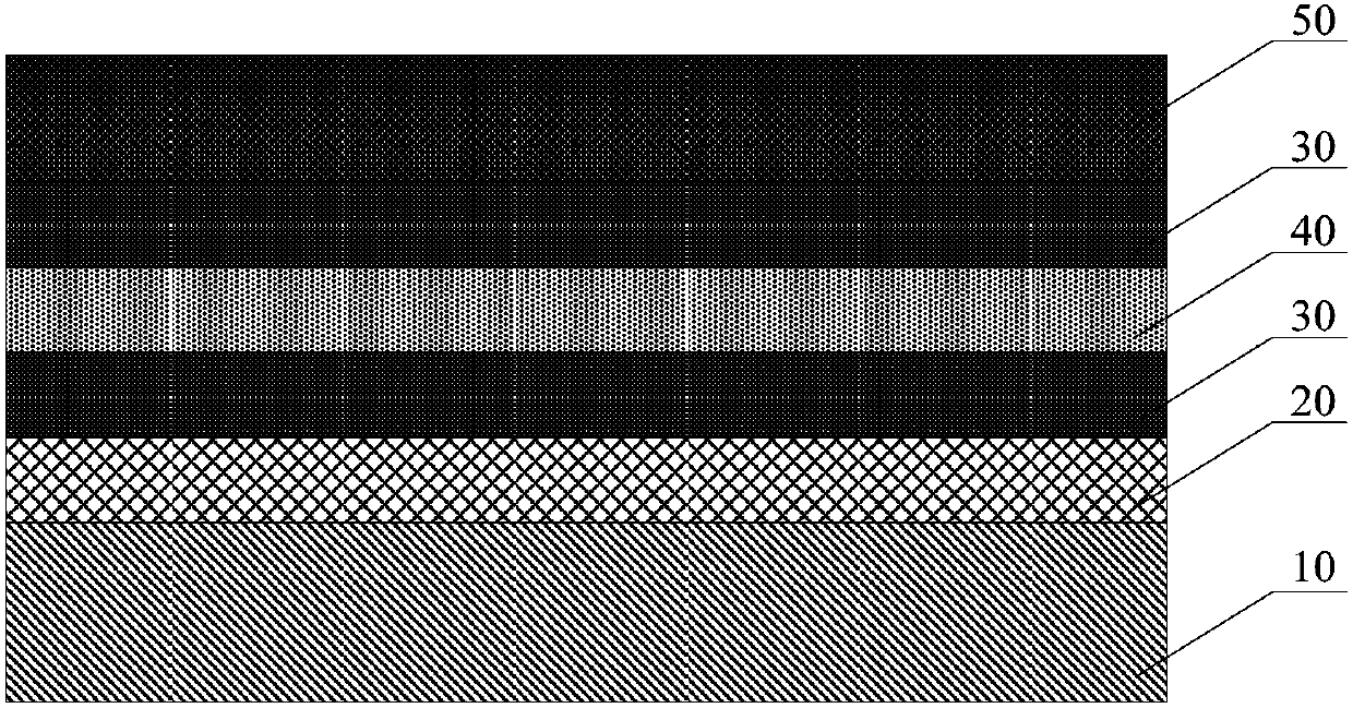
[0074] see figure 1 , the present invention provides a GaAs-based room-temperature infrared luminescent material based on bismuth, and the GaAs-based room-temperature infrared luminescent material based on bismuth includes at least one element made of In x Ga 1-x As material layer 30 and GaAs 1-y Bi y material layer 40 formed of In x Ga 1-x As / GaAs 1-y Bi y / In x Ga 1-x As equal width symmetrical double quantum well material structure; where, 0<x≤0.3, 0<y≤0.15.
[0075]As an example, the GaAs-based room-temperature infrared luminescent material based on bismuth element further includes a substrate 10, a buffer layer 20, and a GaAs cap layer 50; the buffer layer 20 is located on the surface of the substrate 10, and is located on the quantum The bottom of the well material structure; the GaAs cap layer 50 is located at the top of the quantum well material structure; that is, the GaAs-based room temperature infrared luminescent material based on bismuth element includes ...
Embodiment 2
[0105] see Figure 4 , the present invention provides a GaAs-based room-temperature infrared luminescent material based on bismuth, the GaAs-based room-temperature infrared luminescent material based on bismuth includes at least one element made of In x Ga 1-x As material layer and GaAs 1-y Bi y material layer formed by In x Ga 1-x As / GaAs 1-y Bi y Asymmetric quantum well material structure; where, 0<x≤0.3, 0<y≤0.15.
[0106] As an example, the GaAs-based room-temperature infrared luminescent material based on bismuth element further includes a substrate 10, a buffer layer 20, and a GaAs cap layer 50; the buffer layer 20 is located on the surface of the substrate 10, and is located on the quantum The bottom of the well material structure; the GaAs cap layer 50 is located at the top of the quantum well material structure; that is, the GaAs-based room temperature infrared luminescent material based on bismuth element includes the substrate 10 and the buffer layer from bot...
Embodiment 3
[0132] see Figure 6 , the present invention also provides a GaAs-based room-temperature infrared luminescent material based on bismuth, the GaAs-based room-temperature infrared luminescent material based on bismuth comprising at least one In x Ga 1-x As material layer 30 and GaAs 1-y Bi y material layer 40 formed GaAs 1-y Bi y / In x Ga 1-x As / GaAs 1-y Bi y Unequal width double quantum well material structure; wherein, 0<x≤0.3, 0<y≤0.15.
[0133] As an example, the GaAs-based room-temperature infrared luminescent material based on bismuth element further includes a substrate 10, a buffer layer 20, and a GaAs cap layer 50; the buffer layer 20 is located on the surface of the substrate 10, and is located on the quantum The bottom of the well material structure; the GaAs cap layer 50 is located at the top of the quantum well material structure; that is, the GaAs-based room temperature infrared luminescent material based on bismuth element includes the substrate 10 and th...
PUM
 Abstract
Description
Claims
Application Information
 - R&D
- Intellectual Property
- Life Sciences
- Materials
- Tech Scout
- Unparalleled Data Quality
- Higher Quality Content
- 60% Fewer Hallucinations
Browse by: Latest US Patents, China's latest patents, Technical Efficacy Thesaurus, Application Domain, Technology Topic, Popular Technical Reports.
© 2025 PatSnap. All rights reserved.Legal|Privacy policy|Modern Slavery Act Transparency Statement|Sitemap|About US| Contact US: help@patsnap.com


