Board inspection method

A substrate detection and substrate technology, which is applied in the direction of measuring electricity, measuring devices, measuring electrical variables, etc., can solve the problem of not shortening the detection time, etc., and achieve the effect of simple and easy substrate detection, easy substrate detection, and reduced detection times.

Active Publication Date: 2015-12-30
NIDEC-READ CORPORATION
View PDF7 Cites 4 Cited by
  • Summary
  • Abstract
  • Description
  • Claims
  • Application Information

AI Technical Summary

Problems solved by technology

Therefore, even if there are multiple inspection jig heads, it is necessary to perform electrical inspection for each unit substrate, so the inspection time cannot be shortened.

Method used


Image

  • Board inspection method
  • Board inspection method
  • Board inspection method

Examples


Embodiment Construction

[0025] Now, the best mode for carrying out the present invention will be described.

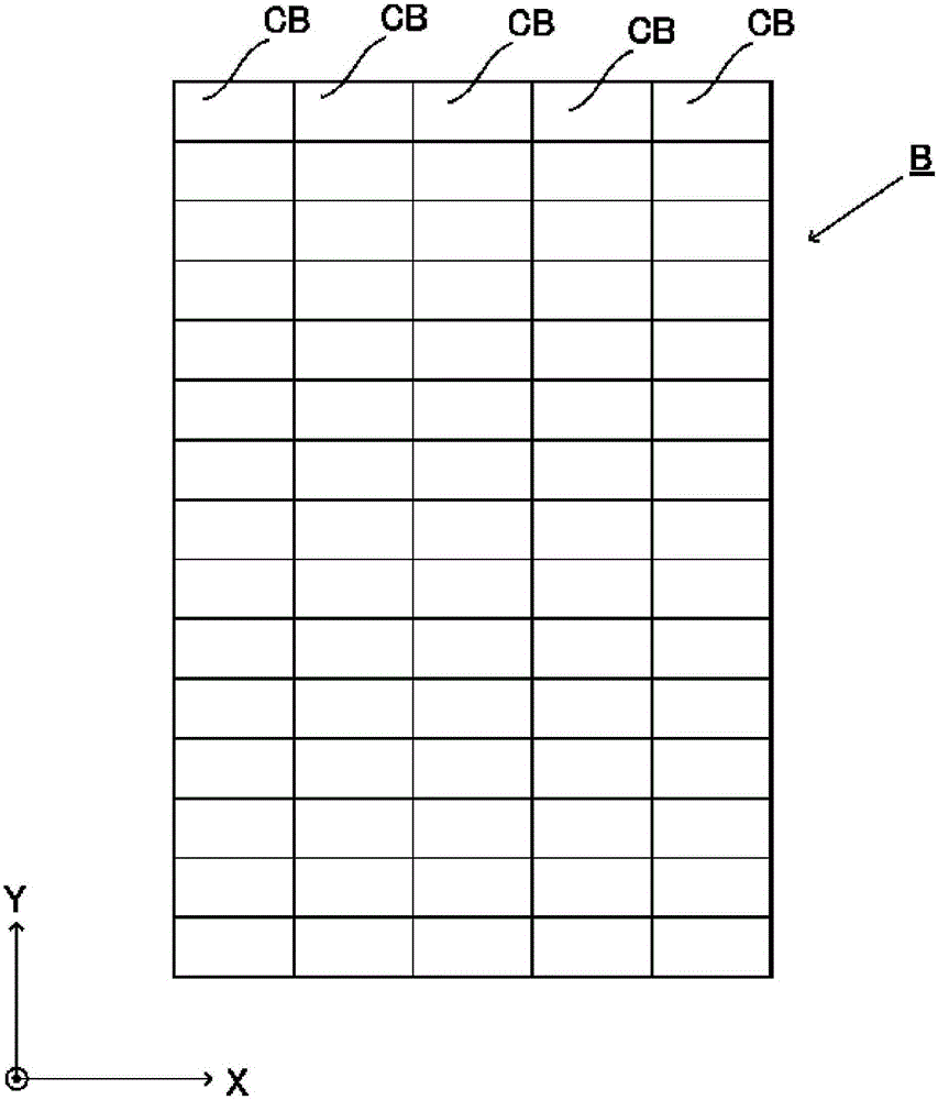
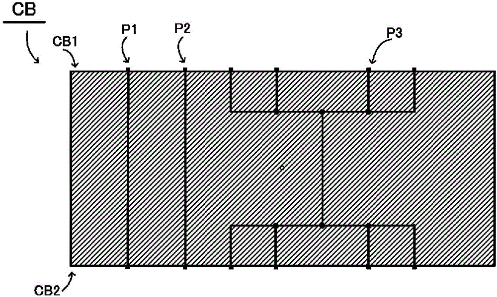
[0026] An object of the present invention is to efficiently perform detection of a sheet substrate B connected by a plurality of unit substrates CB on which one or more wiring patterns P having multiple terminals are formed. Therefore, the sheet substrate B to be detected will be described.

[0027] figure 1 One embodiment of the sheet substrate B is shown. figure 1 The illustrated sheet substrate B is formed in a sheet shape by arranging a plurality of unit substrates CB on which a plurality of wiring patterns are formed in a matrix. The substrate B, as figure 1 As shown, a plurality of unit substrates CB to be detected are formed in a matrix shape with multiple rows and multiple columns. This board|substrate B is divided into each unit board|substrate CB after detection processing etc. are performed. Each unit substrate CB is formed to have a plurality of similar wiring patterns. figu...


PUM


Abstract

An inspection method that reduces the number of times an inspection is performed on multi-terminal wiring patterns is provided. A board inspection method is a method for inspecting wiring patterns of a sheet board that includes a plurality of unit boards, each having a plurality of multi-terminal wiring patterns, by connecting wiring patterns of at least two of the unit boards to a board inspection apparatus for performing electrical inspection, to determine quality of the wiring patterns. The method includes selecting one wiring pattern that is formed on one unit board and is targeted for inspection and another wiring pattern that is formed on another unit board in the same manner as the one wiring pattern, electrically connecting an arbitrary terminal of the one wiring pattern and an arbitrary terminal of the other wiring pattern to establish a short circuit between the one wiring pattern and the other wiring pattern, and performing an inspection for continuity between a terminal other than the arbitrary terminal of the one wiring pattern and a terminal other than the arbitrary terminal of the other wiring pattern.

Description

technical field [0001] The present invention relates to a detection method of a substrate, that is, a substrate detection method, and more specifically, to a substrate detection method that improves the detection tact time when detecting multi-faceted IC packaging substrates. Background technique [0002] Conventionally, wiring formed on a substrate is used to transmit and receive electrical signals to and from ICs and semiconductor components mounted on the substrate, or other electronic components. Such wiring is formed finer and more complex with the recent miniaturization of electronic components, and has lower resistance. As an example of such a substrate, there is a substrate called an IC package substrate. [0003] The IC package substrate is used for electrical connection or fixing of an IC chip and a printed wiring board, or for protecting the IC chip from external dust or the like or moisture. [0004] Such an IC package substrate, as described above, plays the r...

Claims


Application Information

Patent Timeline
Patent Type & Authority Applications(China)
IPC IPC(8): G01R31/02H05K3/00
CPCG01R31/2808G01R1/0433G01R35/00H05K1/0268
Inventor 山下宗宽
Owner NIDEC-READ CORPORATION
Why Eureka
Try Eureka