Solar cell epitaxial wafer and manufacturing method thereof
A technology of a solar cell and a manufacturing method, applied in the field of solar cells, can solve the problems of damage to the cell layer, gas accumulation, and difficulty in discharging, and achieve the effects of preventing damage, reducing time, and improving yield.
- Summary
- Abstract
- Description
- Claims
- Application Information
AI Technical Summary
Problems solved by technology
Method used
Image
Examples
Embodiment 1
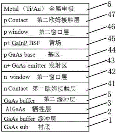
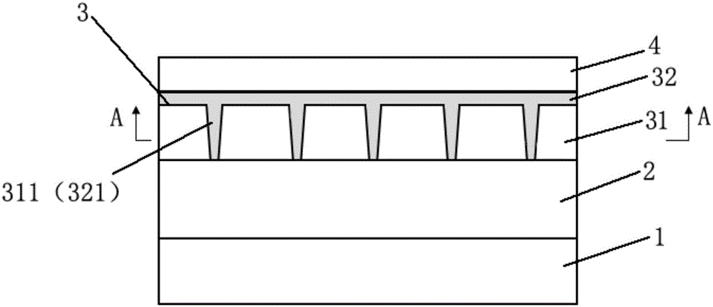
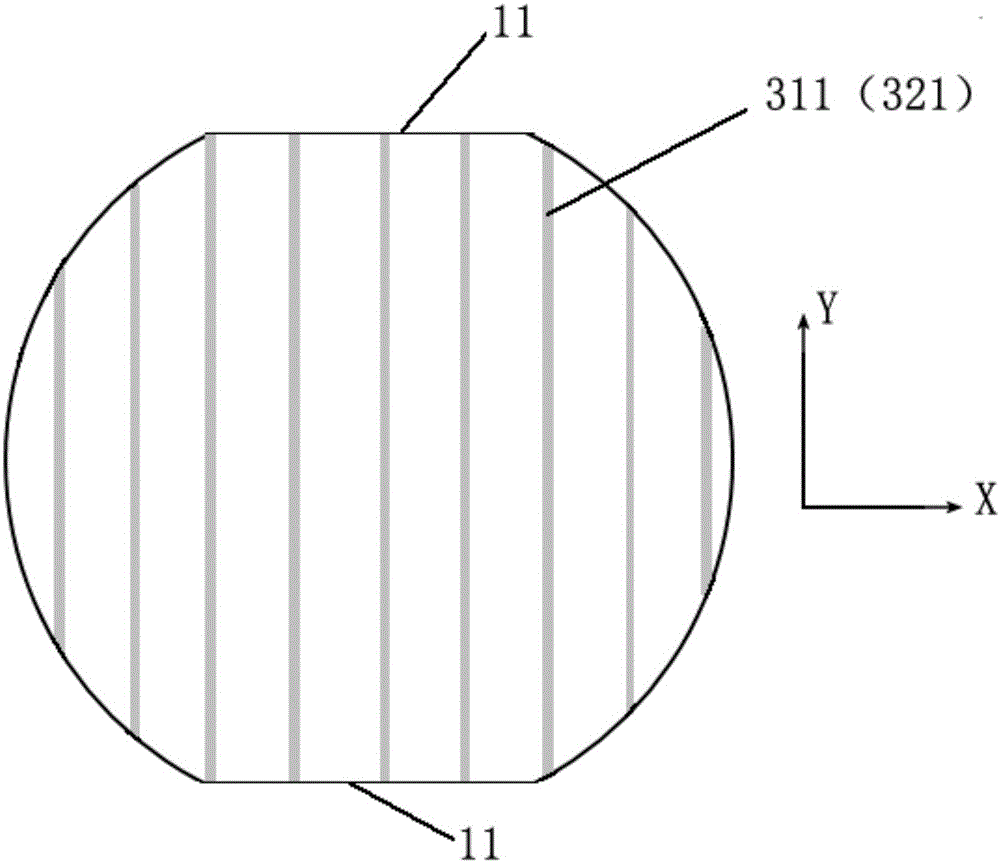
[0039] Such as figure 1 with 2As shown, this embodiment provides a solar cell epitaxial wafer, including a substrate 1, a buffer layer 2, a sacrificial layer 3 and a solar cell layer 4 arranged in sequence, wherein the sacrificial layer 3 includes a first sacrificial layer 31 and a second sacrificial layer 31. Sacrificial layer 32, the first sacrificial layer 31 is arranged close to the buffer layer 2, the second sacrificial layer 32 is arranged close to the first sacrificial layer 31, the etching speed of the first sacrificial layer 31 is greater than the etching speed of the second sacrificial layer 32, A plurality of parallel grooves 311 are distributed on the first sacrificial layer 31 , and the second sacrificial layer 32 has a plurality of protrusions 321 closely fitting with the grooves 311 . figure 2 yes figure 1 Part or all of the sectional view taken along the line A-A of the solar cell epitaxial wafer shown in , wherein the strip-shaped protrusion 321 of the seco...
Embodiment 2
[0057] Such as Figure 7 As shown, the present embodiment provides a method for manufacturing a solar cell epitaxial wafer, comprising the following steps:
[0058] S1: growing the buffer layer 2 epitaxially on the substrate 1, specifically, metal organic compound chemical vapor phase epitaxy (MOCVD) can be used. The metal-organic compound chemical vapor phase epitaxy technology is currently the most mature epitaxial growth technology with the best effect in the manufacture of III-V compound solar cells. In addition, molecular beam epitaxy (MBE) with a slower growth rate can also be selected.
[0059] S2: epitaxially grow the first sacrificial layer 31 on the buffer layer 2, specifically, metal organic compound chemical vapor phase epitaxy (MOCVD) can be used.
[0060] S3: Make a plurality of parallel strip grooves 311 on the first sacrificial layer 31, or make a plurality of holes 312 on multiple parallel straight lines on the first sacrificial layer 31 and on the same line ...
PUM
 Abstract
Description
Claims
Application Information
 - R&D
- Intellectual Property
- Life Sciences
- Materials
- Tech Scout
- Unparalleled Data Quality
- Higher Quality Content
- 60% Fewer Hallucinations
Browse by: Latest US Patents, China's latest patents, Technical Efficacy Thesaurus, Application Domain, Technology Topic, Popular Technical Reports.
© 2025 PatSnap. All rights reserved.Legal|Privacy policy|Modern Slavery Act Transparency Statement|Sitemap|About US| Contact US: help@patsnap.com


