Near-infrared absorbing glass and method for manufacturing same
A near-infrared, manufacturing method technology, applied in TV, color TV, coating, etc., can solve problems such as ghosting, flare, etc., and achieve the effect of preventing ghosting or light spots
- Summary
- Abstract
- Description
- Claims
- Application Information
AI Technical Summary
Problems solved by technology
Method used
Image
Examples
no. 1 Embodiment
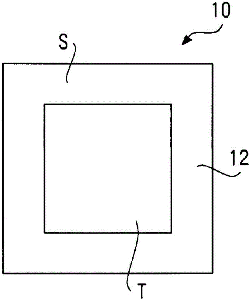
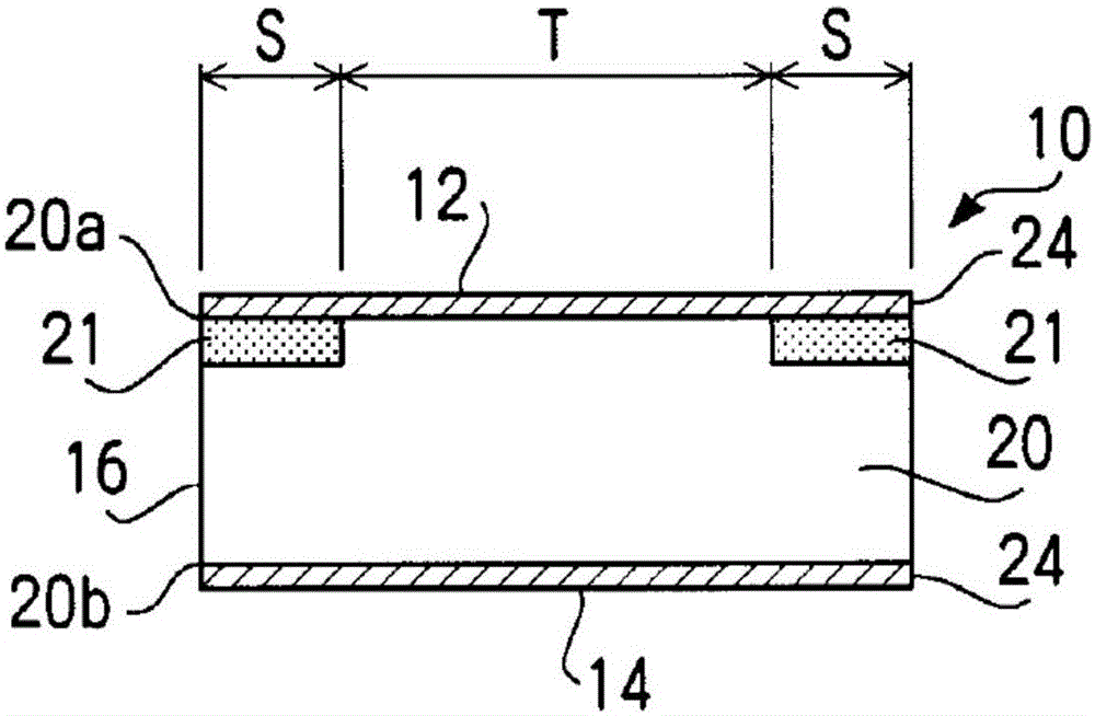
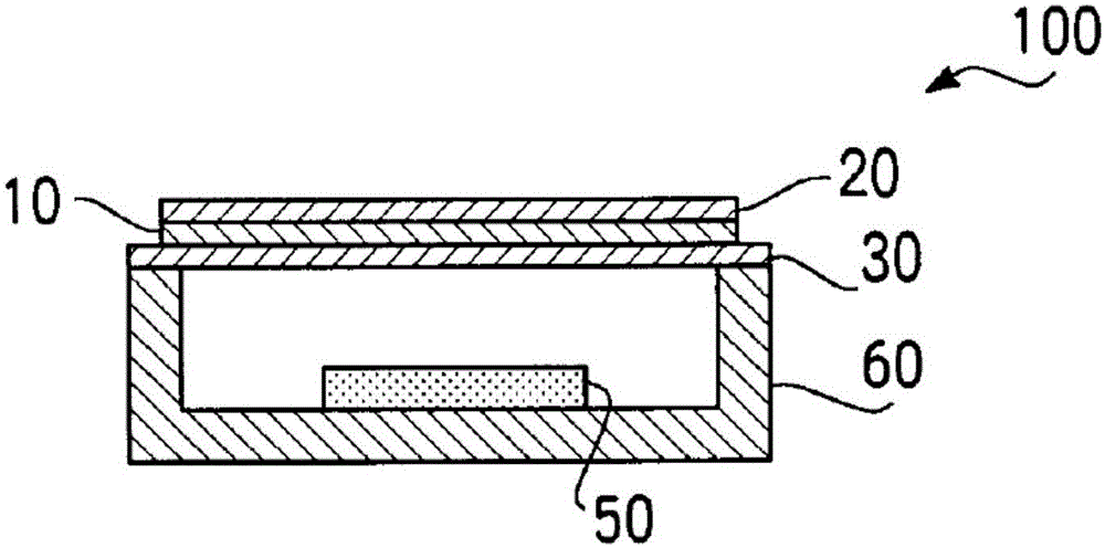
[0044] figure 1 It is a plan view of the near-infrared absorbing glass 10 according to the first embodiment of the present invention. figure 2 It is a side view of the near-infrared absorbing glass 10 according to the first embodiment of the present invention. also, image 3 It is a longitudinal sectional view of the solid-state imaging device 100 in which the opening of the package 60 of the solid-state imaging device 50 is sealed with the near-infrared-absorbing glass 10 according to the first embodiment of the present invention.
[0045] Such as Figure 1 ~ Figure 3 As shown, the near-infrared absorbing glass 10 of this embodiment is disposed between the cover glass 30 of the hermetic package 60 and the low-pass filter 20 for removing ripples of optical analog signals, and absorbs incident light entering the solid-state imaging device 100 Glass for near-infrared rays. The near-infrared absorbing glass 10 is fixed by bonding with a small gap between the cover glass 30 a...
no. 2 Embodiment
[0110] Figure 8 It is a side view of the near infrared absorption glass 10M concerning the 2nd Example of this invention.
[0111] Such as Figure 8As shown, the near-infrared-absorbing glass 10M of this embodiment is different from the near-infrared-absorbing glass 10 of the first embodiment in that a light-shielding layer 23 is provided between the cloudiness layer 21 and the antireflection film 24 .
[0112] The light-shielding layer 23 is a black ink layer with a thickness of about 10 μm formed by screen printing, and is formed on the cloudy layer 21 to block unnecessary light incident on the surface of the glass substrate 20 (the surface on the incident surface 12 side).
[0113] Figure 9 It is a flow chart showing the manufacturing method of the near infrared absorption glass 10M concerning this Example.
[0114] Such as Figure 9 As shown, the manufacturing method of the near-infrared-absorbing glass 10M of the present embodiment is to perform the printing process...
PUM
| Property | Measurement | Unit |
|---|---|---|
| thickness | aaaaa | aaaaa |
| thickness | aaaaa | aaaaa |
Abstract
Description
Claims
Application Information
 - R&D Engineer
- R&D Manager
- IP Professional
- Industry Leading Data Capabilities
- Powerful AI technology
- Patent DNA Extraction
Browse by: Latest US Patents, China's latest patents, Technical Efficacy Thesaurus, Application Domain, Technology Topic, Popular Technical Reports.
© 2024 PatSnap. All rights reserved.Legal|Privacy policy|Modern Slavery Act Transparency Statement|Sitemap|About US| Contact US: help@patsnap.com


