PID-resistant crystalline silicon cell preparation method
A technology of crystalline silicon cells and silicon substrates, applied in the field of solar cells, can solve the problems that silicon nitride films cannot meet insulation requirements, PID attenuation, component output power decline, etc., achieve good passivation, reduce equipment costs, and reduce Effects of small PID phenomena
- Summary
- Abstract
- Description
- Claims
- Application Information
AI Technical Summary
Problems solved by technology
Method used
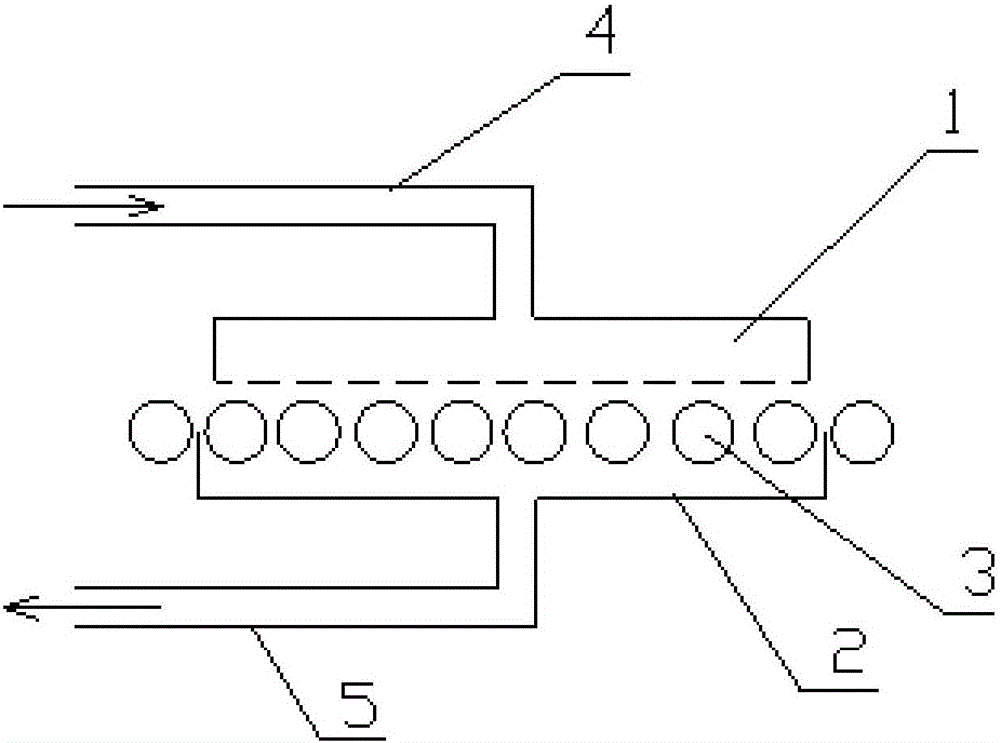
Image

Examples
Embodiment 1
[0019] A method for preparing an anti-PID crystalline silicon battery, comprising the steps of:
[0020] 1) The silicon substrate is cleaned, textured, diffused, and wet-etched;
[0021] 2) oxidizing the silicon substrate after wet etching through an ozone nitrogen gas mixture with an ozone concentration of 30ppm to form a silicon dioxide film on the silicon substrate;
[0022] 3) Deposit a layer of Si with a thickness of 80 nm and a refractive index of 2.01 on the surface of the silicon substrate treated in step 2) using PECVD equipment. 3 N 4 membrane;
[0023] 4) After screen printing and sintering, an anti-PID crystalline silicon battery is obtained, which is marked as 1#.
[0024] Wherein, the ozone nitrogen gas mixture in step 2) is sprayed onto the surface of the silicon substrate, the gas flow rate is 30 L / min, the passing speed of the silicon wafer is 2.3 m / min, and the reaction temperature is 50°C.
Embodiment 2
[0026] A method for preparing an anti-PID crystalline silicon battery, comprising the steps of:
[0027] 1) The silicon substrate is cleaned, textured, diffused, and wet-etched;
[0028] 2) oxidizing the silicon substrate after wet etching through an ozone nitrogen gas mixture with an ozone concentration of 35ppm to generate a layer of silicon dioxide film on the silicon substrate;
[0029] 3) Deposit a layer of Si with a thickness of 82.7 nm and a refractive index of 2.05 on the surface of the silicon substrate treated in step 2) using PECVD equipment. 3 N 4 membrane;
[0030] 4) After screen printing and sintering, an anti-PID crystalline silicon battery is obtained, which is marked as 2#.
[0031] Wherein, the ozone-nitrogen gas mixture in step 2) is sprayed onto the surface of the silicon substrate, the gas flow rate is 40 L / min, the passing speed of the silicon wafer is 2.1 m / min, and the reaction temperature is 55°C.
Embodiment 3
[0033] A method for preparing an anti-PID crystalline silicon battery, comprising the steps of:
[0034] 1) The silicon substrate is cleaned, textured, diffused, and wet-etched;
[0035] 2) oxidizing the silicon substrate after wet etching through an ozone-nitrogen gas mixture with an ozone concentration of 50 ppm to form a silicon dioxide film on the silicon substrate;
[0036] 3) Deposit a layer of Si with a thickness of 83 nm and a refractive index of 2.07 on the surface of the silicon substrate treated in step 2) using PECVD equipment. 3 N 4 membrane;
[0037] 4) After screen printing and sintering, an anti-PID crystalline silicon battery is obtained, which is marked as 3#.
[0038] Wherein, the ozone-nitrogen gas mixture in step 2) is sprayed onto the surface of the silicon substrate, the gas flow rate is 40 L / min, the passing speed of the silicon wafer is 2.2 m / min, and the reaction temperature is 65° C.
PUM
 Abstract
Description
Claims
Application Information
 - R&D
- Intellectual Property
- Life Sciences
- Materials
- Tech Scout
- Unparalleled Data Quality
- Higher Quality Content
- 60% Fewer Hallucinations
Browse by: Latest US Patents, China's latest patents, Technical Efficacy Thesaurus, Application Domain, Technology Topic, Popular Technical Reports.
© 2025 PatSnap. All rights reserved.Legal|Privacy policy|Modern Slavery Act Transparency Statement|Sitemap|About US| Contact US: help@patsnap.com