High voltage power device and method of forming the same
A high-voltage power device and device technology, which is applied in semiconductor devices, semiconductor/solid-state device manufacturing, electrical components, etc., can solve problems such as monotonous concentration, increased device on-resistance, and reduced device current capability
- Summary
- Abstract
- Description
- Claims
- Application Information
AI Technical Summary
Problems solved by technology
Method used
Image
Examples
no. 1 example
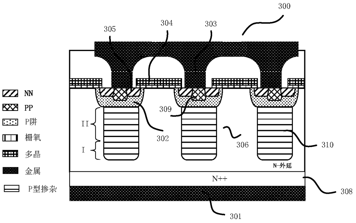
[0129] refer to image 3 , image 3 The shown high-voltage power device 300 is a high-voltage MOS device, which mainly includes: an N-type first doped region 306 located on an N-type doped substrate 308; a first electrode 301 connected to the first doped region via the substrate 308 The impurity region 306 is in electrical contact; a plurality of P-type well regions 302 are arranged laterally in the upper surface of the first doped region 306; the P-type second doped region 310 has one end connected to the well region 302 and the other end Extend vertically into the first doped region 306; the N-type device doped region 305 and the P-type device doped region 309 are formed in the well region 302, and the second doped region 310 is connected to the P-type doped region through the well region 302. The device doping region 309 is in electrical contact; the gate 304 is formed on the upper surface of the first doping region 306; the second electrode 303 is in contact with the N-ty...
no. 2 example
[0136] refer to Figure 4 , Figure 4 The shown high-voltage power device 400 is a high-voltage MOS device, and its structure is the same as image 3 Basically the same, including: an N-type first doped region 406 located on an N-type doped substrate 408; a first electrode 401 electrically contacting the first doped region 406 through the substrate 408; a plurality of P-type The well region 402 is horizontally arranged in the upper surface of the first doped region 406; the P-type second doped region 410 has one end connected to the well region 402, and the other end extends vertically into the first doped region 406; The N-type device doping region 405 and the P-type device doping region 409 are formed in the well region 402, and the second doping region 410 is in electrical contact with the P-type device doping region 409 via the well region 402; the gate 404 is formed on the upper surface of the first doped region 406 ; the second electrode 403 is in electrical contact wi...
no. 3 example
[0154] refer to Figure 12 , Figure 12 The shown high-voltage power device 800 is a high-voltage MOS device, and its structure is the same as image 3 Basically the same, including: an N-type first doped region 806 located on an N-type doped substrate 808; a first electrode 801 electrically contacting the lower surface of the first doped region 806 via the substrate 808; a plurality of The P-type well region 802 is horizontally arranged in the upper surface of the first doped region 806; the P-type second doped region 810 is connected to the well region 802 at one end and extends vertically to the first doped region at the other end. 806; the N-type device doping region 805 and the P-type device doping region 809 are formed in the well region 802, and the second doping region 810 is in electrical contact with the P-type device doping region 809 via the well region 802 The gate 804 is formed on the upper surface of the first doped region 806 ; the second electrode 803 is in ...
PUM
 Abstract
Description
Claims
Application Information
 - R&D
- Intellectual Property
- Life Sciences
- Materials
- Tech Scout
- Unparalleled Data Quality
- Higher Quality Content
- 60% Fewer Hallucinations
Browse by: Latest US Patents, China's latest patents, Technical Efficacy Thesaurus, Application Domain, Technology Topic, Popular Technical Reports.
© 2025 PatSnap. All rights reserved.Legal|Privacy policy|Modern Slavery Act Transparency Statement|Sitemap|About US| Contact US: help@patsnap.com


