Fin field effect transistor and formation method thereof

A fin-type field effect and transistor technology, which is applied in semiconductor devices, semiconductor/solid-state device manufacturing, electrical components, etc., can solve the problems of low mobility and low saturation current of PMOS transistors, and achieve high mobility and hole-carrying current Improvement of sub-mobility, effect of performance improvement

Active Publication Date: 2015-11-25
SEMICON MFG INT (SHANGHAI) CORP
View PDF5 Cites 10 Cited by
  • Summary
  • Abstract
  • Description
  • Claims
  • Application Information

AI Technical Summary

Problems solved by technology

[0005] For P-type fin field effect transistors, because the carriers of P-type fin field effect transistors are holes, and the mobility of holes in silicon is low, resulting in low saturation current of PMOS transistors.
[0006] The performance of the P-type fin field effect transistor needs to be further improved

Method used


Image

  • Fin field effect transistor and formation method thereof
  • Fin field effect transistor and formation method thereof
  • Fin field effect transistor and formation method thereof

Examples


Embodiment Construction

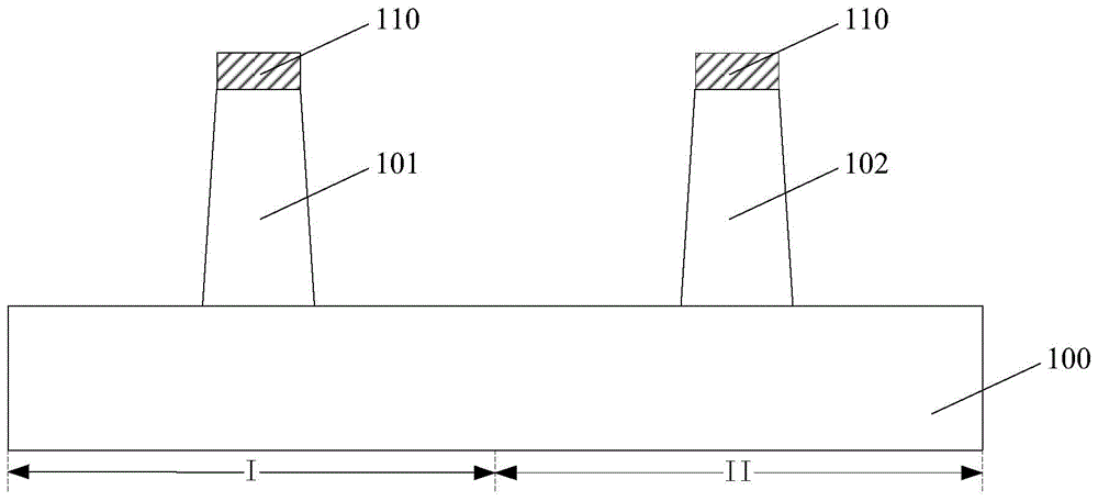
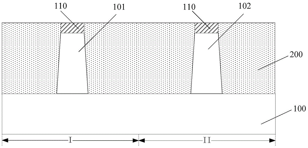
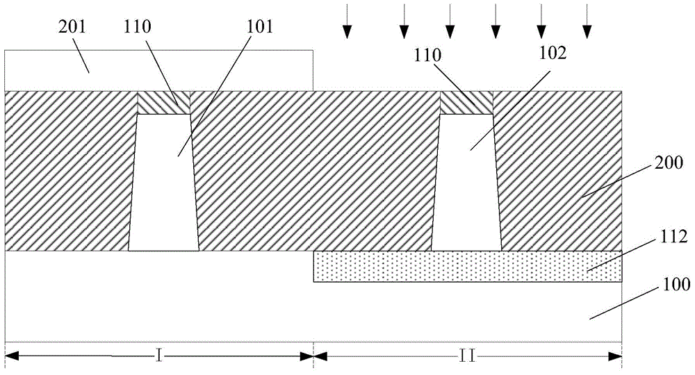
[0033] As mentioned in the background art, the performance of the P-type fin field effect transistor formed in the prior art needs to be further improved.

[0034] Studies have found that the migration rate of hole carriers in germanium or germanium-silicon materials in P-type fin field effect transistors is greater than that in silicon, and using germanium or germanium-silicon materials as fin materials can improve the performance of P-type fin field effect transistors. The hole mobility of the P-type fin field effect transistor, thereby improving the performance of the P-type fin field effect transistor. In one embodiment, a germanium layer or a silicon germanium layer may be formed by epitaxy on a substrate, and then the germanium layer or silicon germanium layer may be etched to serve as the channel region of the P-type fin field effect transistor. However, the yield of the single-crystal germanium layer formed by the epitaxial process is low and the cost is high, and ther...


PUM

PropertyMeasurementUnit
Heightaaaaaaaaaa
Thicknessaaaaaaaaaa

Abstract

The invention relates to a fin field effect transistor and a formation method thereof. The formation method of the fin field effect transistor comprises the steps of providing a semiconductor substrate; forming a first pin portion on the semiconductor substrate; forming an isolation material layer whose surface is flush with the top surface of the first fin portion on the semiconductor substrate; carrying out mobility enhancement ion implantation on the first fin portion, and forming an implantation region at the top end of the first fin portion; carrying out local recrystallization treatment on the implantation region, and enabling the implantation region to become a single crystal semiconductor layer containing implanted ions, wherein a hole mobility of the single crystal semiconductor layer is greater than the hole mobility of the first fin portion below the single crystal semiconductor layer; etching the isolation material layer, and forming an isolation layer whose surface is flush with the bottom surface of the single crystal semiconductor layer; and forming a first grid structure crossing the single crystal semiconductor layer. The method provided by the invention can improve the performance of the formed fin field effect transistor.

Description

technical field [0001] The invention relates to the technical field of semiconductors, in particular to a fin field effect transistor and a forming method thereof. Background technique [0002] With the continuous development of semiconductor process technology, the process node is gradually reduced, and the gate-last (gate-last) process has been widely used to obtain an ideal threshold voltage and improve device performance. However, when the feature size of the device is further reduced, even if the gate-last process is adopted, the structure of the conventional MOS field effect transistor can no longer meet the requirements for device performance, and the fin field effect transistor (FinFET) has been obtained as a multi-gate device. Widespread concern. [0003] The fin field effect transistor in the prior art generally uses silicon as the fin material, that is, the material of the channel region of the fin field effect transistor is silicon. [0004] Since the carriers ...

Claims


Application Information

Patent Timeline
IPC IPC(8): H01L21/336H01L21/265H01L29/78
Inventor 三重野文健
Owner SEMICON MFG INT (SHANGHAI) CORP
Why Eureka
Try Eureka