
Method for detecting content of substitutional carbon and interstitial oxygen in monocrystalline silicon

A technology for substituting carbon and single crystal silicon, which is used in measurement devices, material analysis by optical means, instruments, etc., can solve the problems of unmeasurable substituted carbon and interstitial oxygen content, and achieves reduction of interference fringes, improvement of measurement accuracy, reduction of Scattering effect

Inactive Publication Date: 2015-11-25
NANJING XIUKE INSTR CO LTD
View PDF3 Cites 9 Cited by
  • Summary
  • Abstract
  • Description
  • Claims
  • Application Information

AI Technical Summary

Problems solved by technology

[0014] Aiming at the problem that in the prior art, the content of substituting carbon and interstitial oxygen in crystalline silicon slices with a thickness of 0.2-2.0mm can be measured, but the content of substituting carbon and interstitial oxygen in crystalline silicon slices with a thickness of 0.1mm-0.2mm cannot be measured. , the present invention proposes a method for measuring the content of substituent carbon and interstitial oxygen in single crystal silicon

Method used


Image

  • Method for detecting content of substitutional carbon and interstitial oxygen in monocrystalline silicon
  • Method for detecting content of substitutional carbon and interstitial oxygen in monocrystalline silicon
  • Method for detecting content of substitutional carbon and interstitial oxygen in monocrystalline silicon

Examples


Embodiment 1

[0060] Taking the measurement of substituent carbon and interstitial oxygen content of single crystal silicon produced by China Shanghai Junhe Electronic Materials Co., Ltd. as an example, the content of the present invention will be described in detail. The thickness of the sample silicon wafer is 100 μm, the silicon wafer is cut into a rectangle, 1.6cm×5cm, the crystal type is , the doping type is n-type, phosphorus doped, and the resistivity is 15Ω·cm silicon wafer, referred to as CZ silicon wafer ; The reference silicon wafer does not contain carbon and oxygen, and its resistivity is 3000Ω·cm. The rest is the same as the sample silicon wafer, referred to as FZ silicon wafer. The flatness is less than 1 / 4 of the wavelength of the incident infrared light to avoid the influence of silicon lattice vibration in the carbon absorption band, and the transmittance at the absorption peak is not lower than 20% to reduce the scattering of infrared light. Application No. 200610097859.4...

Embodiment 2

[0114] The thickness of the sample silicon wafer is 200 μm, the rest of the parameters of the sample silicon wafer and the reference silicon wafer, the detection method and steps are the same as in Example 1, and Table 2 shows the carbon and oxygen content in the 200 μm silicon wafer measured by the MTR-IR method.

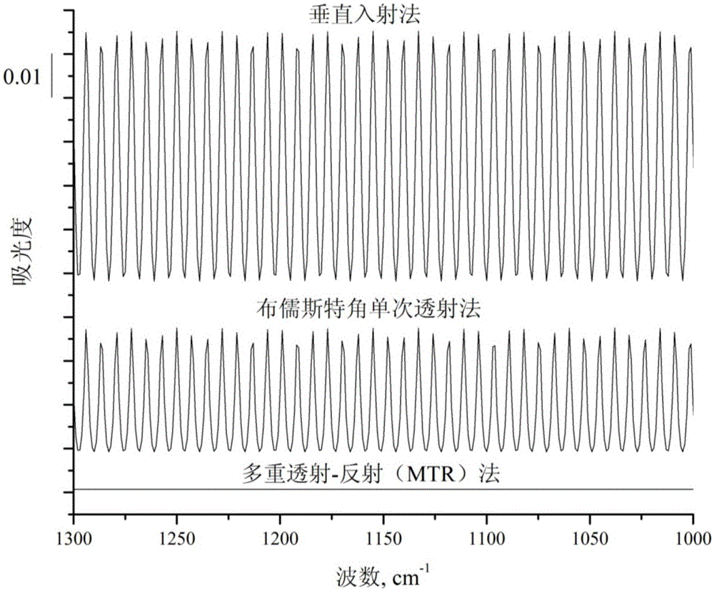
[0115] Interference reduction effect of Brewster's angle

[0116] Figure 11 It is a schematic diagram of the multiple transmission-reflection (MTR) accessory and the infrared light path; figure 1 is a schematic diagram of the optical path of P-polarized light transmission and reflection, figure 1 From top to bottom in the figure are the gold mirror, the silicon wafer and the gold mirror. In the lower left corner of the figure, the incident light, that is, the p-polarized light in the figure, is incident on the surface of the silicon wafer at the Brewster angle (ie 74°), and passes through the silicon wafer. It reaches the reflection on the gold mirror at the t...

Embodiment 3

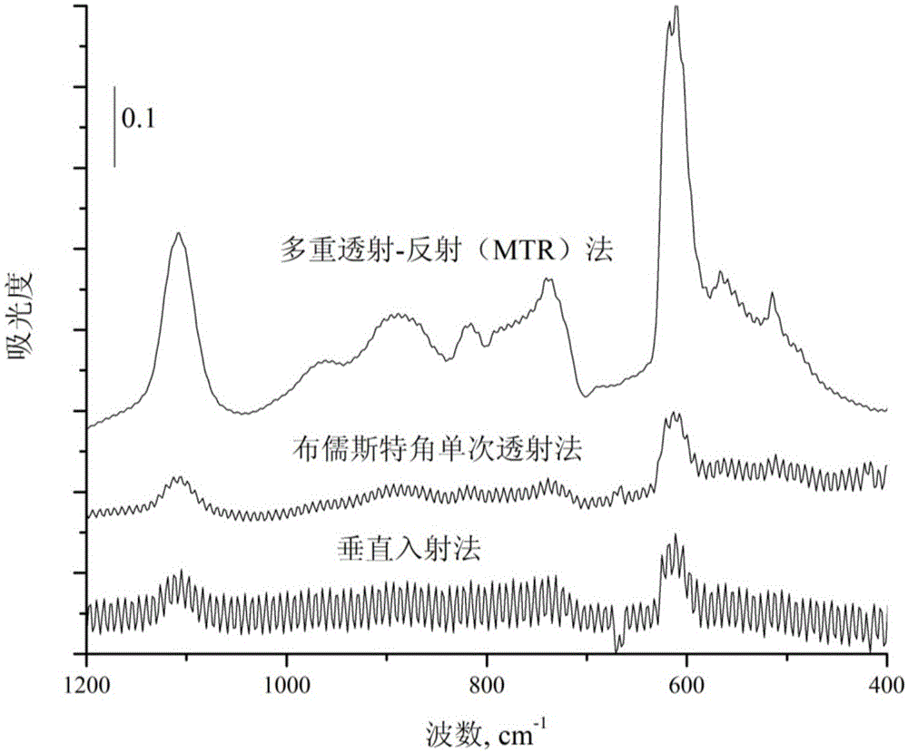
[0125] Except that the thickness of the sample and the reference silicon wafer is 450 μm, other parameters, detection methods and steps are the same as in Example 1. Image 6 Among them, MTR-sample represents the spectrogram of the sample silicon wafer measured by the MTR-IR method; IR-sample represents the spectrogram of the sample silicon wafer measured by the vertical incidence IR method, the sample length is 5cm, n=3.42, N=10, b=0.0450 cm,b B =0.0469cm,b TMR = 0.469 cm, incident angle = 74°. Image 6 The infrared spectra of the MTR-IR method and the vertical incidence IR method of the same silicon wafer are given. By comparison, it can be seen that the sample absorbance of the MTR-IR method is always greater than that of the vertical incidence IR method, especially at the gap oxygen peak 1107cm -1 and substituting carbon peak 605cm -1 , the contrast between the MTR-IR method and the vertical incidence IR method in terms of peak height or peak area is very obvious. In the ...


PUM

PropertyMeasurementUnit
thicknessaaaaaaaaaa
electrical resistivityaaaaaaaaaa

Abstract

The invention discloses a method for detecting the content of substitutional carbon and interstitial oxygen in monocrystalline silicon, and belongs to the field of semiconductor material examination and analysis. The method includes the steps that a reference silicon wafer and a sample silicon wafer are placed on a sample fixing rack for repeated transmission-reflection measuring accessories, and p-linear polarization infrared beams are used for executing N times of the transmission-reflection process; the p-linear polarization infrared beams arrive at an infrared detector, infrared absorption spectrograms are obtained, the difference value of the absorbance of the position where the absorption peak of the substitutional carbon and the interstitial oxygen on the infrared spectrogram of the sample silicon wafer is located and the absorbance of the position where the absorption peak of the substitutional carbon and the interstitial oxygen on the infrared spectrogram of the reference silicon wafer is located is calculated, namely the absorbance of the substitutional carbon and the interstitial oxygen in the sample silicon wafer is obtained; the concentration of the substitutional carbon and the interstitial oxygen can be obtained according to the one-time Brewster infrared transmission equation and the Lambert-Beer law. By the adoption of the method, the monocrystalline silicon with the thickness being 0.1-2.0 mm can be measured, and the measuring accuracy is high.

Description

technical field [0001] The invention relates to the field of inspection and analysis of semiconductor materials, in particular to a method for measuring the content of substituting carbon and interstitial oxygen in single crystal silicon. Background technique [0002] Silicon is the largest and most widely used semiconductor material today. Its output and usage mark the R&D and production level of a country's electronics and solar energy industries. The production and testing technology of high-quality silicon materials and the high technology of silicon-based devices promote each other. Such as 1) The semiconductor industry based on silicon is a miracle in human history. Its appearance has revolutionized all aspects of human life, from mobile phones, communications, computers and their networks that accompany us in daily life to intelligent production and transportation systems such as digital Machine tools, automobiles, high-speed rail, and aircraft controls are all based...

Claims


Application Information

Patent Timeline
Patent Type & Authority Applications(China)
IPC IPC(8): G01N21/3563
Inventor 肖守军路小彬
Owner NANJING XIUKE INSTR CO LTD
Learn More