Packaging substrate and fabrication method thereof
By arranging an alignment layer between the metal pillars and the conductive blind holes of the packaging substrate, the problems of poor plating effect and complicated manufacturing steps caused by the large aspect ratio of the metal pillars in the existing technology are solved, and high-density wiring and component settings are achieved. , enhancing the overall yield and adhesion.
- Summary
- Abstract
- Description
- Claims
- Application Information
AI Technical Summary
Problems solved by technology
Method used
Image

Examples
no. 1 example
[0046] Figure 3A to Figure 3N What is shown is a cross-sectional view of the first embodiment of the manufacturing method of the packaging substrate of the present invention.
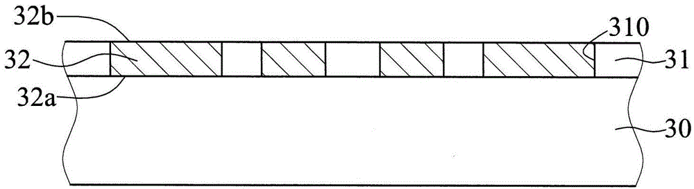
[0047] like Figure 3A As shown, a first resistive layer 31 having a first opening 310 is formed on the top surface of a carrier board 30, and a first resisting layer 31 having an opposite first surface 32a and a second surface 32b is formed in the first opening 310. A conductive part 32 is used to connect the first conductive part 32 to the supporting board 30 through its first surface 32a, and the supporting board 30 can be a steel plate.
[0048] like Figure 3B As shown, a second resistive layer 33 with a second opening 330 is formed on the first resistive layer 31 and the first conductive portion 32, and the second resistive layer 33 of the first conductive portion 32 in the second opening 330 Metal posts 34 are formed on surface 32b.
[0049] like Figure 3C As shown, on the end surface of t...
no. 2 example
[0065] Figure 4A to Figure 4D What is shown is a cross-sectional view of the second embodiment of the manufacturing method of the packaging substrate of the present invention.
[0066] This embodiment is substantially similar to the previous embodiment, with the main differences described below.
[0067] like Figure 4A shown, which continues from Figure 3E , grinding the package body 37, so that the alignment layer 35 is embedded and flush with the fourth surface 37b.
[0068] like Figure 4B As shown, a dielectric material 45 is formed on the fourth surface 37 b and the alignment layer 35 , and the material of the dielectric material 45 can be polyimide or a molding compound.
[0069] like Figure 4C As shown, part of the dielectric material 45 is removed to form a blind hole 450 exposing part of the alignment layer 35 .
[0070] like Figure 4D As shown, a conductive blind hole 46 is formed in the blind hole 450 on the alignment layer 35, and a second conductive po...
PUM
 Abstract
Description
Claims
Application Information
 - R&D
- Intellectual Property
- Life Sciences
- Materials
- Tech Scout
- Unparalleled Data Quality
- Higher Quality Content
- 60% Fewer Hallucinations
Browse by: Latest US Patents, China's latest patents, Technical Efficacy Thesaurus, Application Domain, Technology Topic, Popular Technical Reports.
© 2025 PatSnap. All rights reserved.Legal|Privacy policy|Modern Slavery Act Transparency Statement|Sitemap|About US| Contact US: help@patsnap.com