IGBT (Insulated Gate Bipolar Transistor) chip manufacturing method for crimped type package

A manufacturing method and crimping technology, which is applied in semiconductor/solid-state device manufacturing, electrical components, transistors, etc., can solve problems such as high process precision requirements, high processing costs, and extended chip processing cycle, and achieve low process precision requirements , save the cost of tape-out, and ensure the effect of electrical characteristics

Active Publication Date: 2015-07-29
GLOBAL ENERGY INTERCONNECTION RES INST CO LTD +1
View PDF5 Cites 6 Cited by
  • Summary
  • Abstract
  • Description
  • Claims
  • Application Information

AI Technical Summary

Problems solved by technology

In terms of the conventional semiconductor process flow, there are two options to choose: first, after the metal electrode is completed, the second metal deposition, photolithography process, and metal etching are performed to complete, but this method needs to be completed in the second Before layer metal deposition, a corrosion barrier layer (usually Si x N y ), it is necessary to add a photolithography process, which leads to the extension of the chip processing cycle and the increase of the processing cost; second, the direct deposition of thick metal is completed by two photolithography processes and metal etching, but because metal etching is generally a wet process Etching, the thickness of the two layers of metal is not easy to control, and the process precision is high

Method used


Image

  • IGBT (Insulated Gate Bipolar Transistor) chip manufacturing method for crimped type package
  • IGBT (Insulated Gate Bipolar Transistor) chip manufacturing method for crimped type package

Examples


Embodiment 1

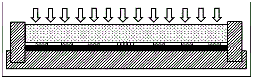
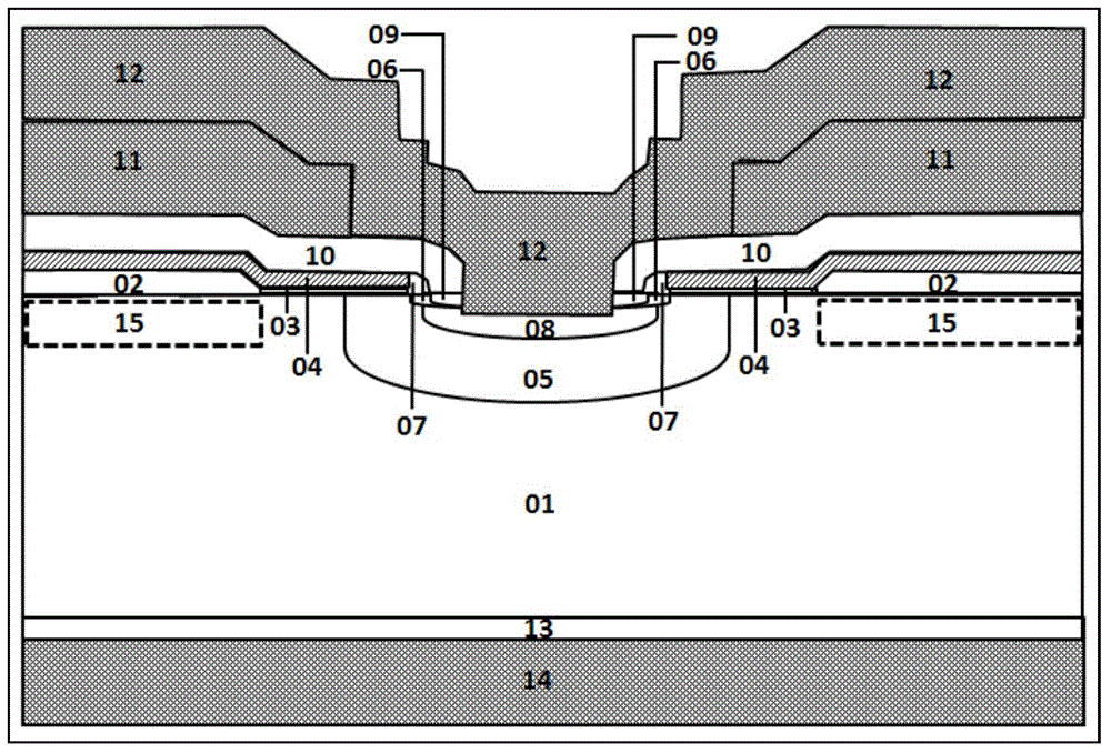
[0034] The invention of this example provides a method for manufacturing an IGBT chip suitable for press-fit packaging, including: figure 2 as shown,

[0035] (1) N-type single crystal silicon wafer substrate 1, the doping concentration of the substrate N impurity and the thickness of the substrate need to be selected according to different breakdown voltage and forward conduction voltage drop requirements (600V to 6500V). Alkali, deionized water ultrasonic cleaning and other processes are used to chemically treat the silicon surface.

[0036] (2) Field oxide layer 2 growth and etching: use high temperature oxidation to grow an oxide layer on the surface of the silicon wafer with a thickness of 1000-1500nm. After the growth is completed, perform photolithography and wet etching. The smoother the etching angle of the oxide layer The better, the final angle is about 30°, and the field oxygen is 10-12μm away from the polycrystalline opening.

[0037] (3) Fabrication of chip pl...


PUM


Abstract

The invention relates to an IGBT (Insulated Gate Bipolar Transistor) chip manufacturing method for crimped type package. The IGBT chip manufacturing method comprises the following steps: selecting a silicon substrate and preprocessing the silicon substrate; carrying out field oxide layer growth on the surface of the silicon substrate, and etching the field oxide layer; manufacturing a gate oxide layer and a polysilicon gate electrode; manufacturing a P well and an N well; manufacturing Spacer, a P+ type doping region and an N+ type doping region; forming a positive electrode EM2 above the polysilicon gate electrode; forming a positive electrode EM1 on the outer side of the positive electrode EM2; forming a P+ collector region on the back surface of the silicon substrate; manufacturing a back electrode C. According to the technical scheme provided by the invention, the IGBT chip manufacturing method has low requirement on technological precision, and the tape-out cost is reduced.

Description

Technical field: [0001] The invention relates to the field of power electronic devices, and more specifically relates to a method for manufacturing an IGBT chip suitable for crimping packaging. Background technique: [0002] The structural form of the press-fit IGBT is derived from the packaging form of traditional power devices such as thyristors and GTOs. It does not require chip welding, avoids the binding of leads, and can reduce the parasitic inductance of the circuit; the press-fit IGBT module can dissipate heat on both sides, and the heat dissipation efficiency Higher and better reliability; based on the fact that the crimping IGBT module is easy to be connected in series, the voltage level of the equipment can be improved. With this feature, the crimping module is widely used in ultra-high voltage (HVDC), static var compensation (SVC), multi- Level inverters, etc.; in addition, the short-circuit failure mode of the crimped IGBT module makes the power grid more stable...

Claims


Application Information

Patent Timeline
Patent Type & Authority Applications(China)
IPC IPC(8): H01L21/331H01L21/28
CPCH01L29/0649H01L29/401H01L29/41H01L29/66325H01L29/66333
Inventor 高明超王耀华赵哿刘江李立金锐温家良
Owner GLOBAL ENERGY INTERCONNECTION RES INST CO LTD
Why Eureka
Try Eureka