Photodetector and preparation method based on graphene and nanostructure perovskite material

A technology of perovskite materials and nanostructures, applied in semiconductor/solid-state device manufacturing, photovoltaic power generation, electric solid-state devices, etc., can solve the problems of inapplicability, device size limit, and difficulty in realizing ultrafast broadband absorption photodetectors, etc. Achieve the effect of improving device responsivity, high device success rate and good compatibility

Inactive Publication Date: 2017-05-10
深圳激子科技有限公司
View PDF3 Cites 0 Cited by
  • Summary
  • Abstract
  • Description
  • Claims
  • Application Information

AI Technical Summary

Problems solved by technology

The spectral range and detection bandwidth of conventional photodetectors based on group IV and III-V semiconductors (such as silicon and gallium arsenide) are limited by their energy bands and carrier transit times, making it difficult to achieve ultrafast broadband absorption The optical detector is not suitable for some applications that have stricter requirements on device performance, such as the field of ultra-fast broadband data transmission
On the other hand, as the requirements for device integration increase, the device size needs to be continuously reduced, and the traditional device size based on Group IV and III-V semiconductors is approaching its limit.

Method used


Image

  • Photodetector and preparation method based on graphene and nanostructure perovskite material
  • Photodetector and preparation method based on graphene and nanostructure perovskite material
  • Photodetector and preparation method based on graphene and nanostructure perovskite material

Examples


Embodiment Construction

[0036] The present invention will be described in detail below with reference to the accompanying drawings and in conjunction with the embodiments.

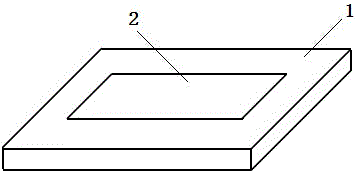
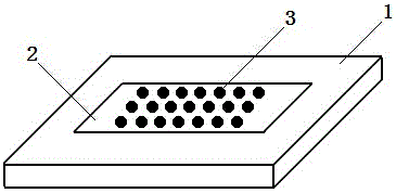
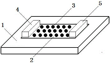
[0037] see Figure 1-6As shown, a photodetector based on graphene and nanostructured perovskite materials includes a silicon substrate 1 covered with silicon dioxide, and the silicon substrate 1 can serve as a gate electrode, and can also be covered by it Silicon dioxide acts as a gate dielectric layer, and the middle part of the upper surface of the silicon substrate 1 is provided with a graphene conductive layer 2, and the middle part of the upper surface of the graphene conductive layer 2 is distributed with several nanostructure organic lead halide perovskite materials Layer 3, the graphene conductive layer 2 and the nanostructure organic lead halide perovskite material layer 3 form a heterojunction structure, and the left and right ends of the upper surface of the graphene conductive layer 2 are respectively provided with fi...


PUM

PropertyMeasurementUnit
thicknessaaaaaaaaaa
thicknessaaaaaaaaaa

Abstract

The invention discloses a photodetector based on graphene and nano-structure perovskite materials and a preparation method, comprising a silicon substrate covered with silicon dioxide, a graphene conductive layer is arranged on the silicon substrate, and the graphene conductive layer The middle part is distributed with a nanostructured organic lead halide perovskite material layer, and forms a heterojunction structure. An electrode layer is provided at the left and right ends of the graphene conductive layer; a passivation layer is provided on the top of the silicon substrate to passivate The graphene conductive layer, the nanostructure organic lead halide perovskite material layer and the two electrode layers are all covered; a contact hole of the electrode is formed by photolithography and etching on the passivation layer above the two electrode layers , metal lead-out electrodes are respectively deposited on the two contact holes. Compared with the current silicon electronic technology platform, the technology for constructing the photodetection device of the present invention has good compatibility, and the preparation process is simple, the success rate of the device is high, and it has great potential to realize fast, broadband response and wide-spectrum photodetection.

Description

technical field [0001] The invention belongs to the field of photodetectors, in particular to a photodetector based on graphene and nanostructure perovskite materials and a preparation method. Background technique [0002] For a photodetector, the detection bandwidth and response speed of the photodetector are important parameters to measure its performance. The spectral range and detection bandwidth of conventional photodetectors based on group IV and group III-V semiconductors (such as silicon and gallium arsenide) are limited by their energy bands and carrier transit times, making it difficult to achieve ultrafast broadband absorption The photodetector is not suitable for some applications with stricter device performance requirements, such as ultra-fast broadband data transmission. On the other hand, with the increasing requirements for device integration, the device size needs to be continuously reduced, and the size of traditional devices based on Group IV and Group I...

Claims


Application Information

Patent Timeline
Patent Type & Authority Patents(China)
IPC IPC(8): H01L51/48H01L51/46H01L51/44H01L51/42
CPCH10K30/00H10K30/30Y02E10/549Y02P70/50
Inventor 鲍桥梁王玉生李绍娟
Owner 深圳激子科技有限公司
Why Eureka
Try Eureka