Near-infrared cut filter and solid-state imaging device
A cut-off filter and near-infrared technology, which can be used in instruments, image communications, televisions, etc., can solve problems such as insufficient permeability and lack of access to near-infrared cut-off filters and optical filters.
- Summary
- Abstract
- Description
- Claims
- Application Information
AI Technical Summary
Problems solved by technology
Method used
Image
Examples
preparation example Construction
[0197] For the preparation of the coating liquid, stirring devices such as a magnetic stirrer, an autorotation / revolution mixer, a bead mill, a planetary mill, and an ultrasonic homogenizer can be used. In order to secure high transparency, it is preferable to sufficiently stir. Stirring can be carried out continuously or intermittently.
[0198] The coating of the coating liquid can be performed by dip coating, cast coating, spray coating, spin coating, bead coating, wire bar coating, knife coating, roll coating, curtain coating, slit coating, etc. Coating methods such as die coating, gravure coating, slot reverse coating, micro gravure printing, inkjet or comma coating. In addition, a bar coating method, a screen printing method, a flexographic printing method, or the like can also be used.
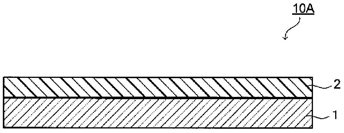
[0199] The near-infrared absorbing layer 2 is formed on the glass substrate 1 by coating the above-mentioned coating liquid on the glass substrate 1 and then drying it. When the coat...
Embodiment
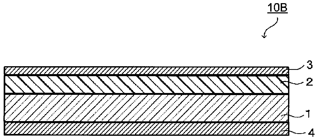
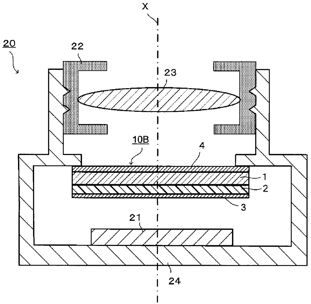
[0240] Hereinafter, the present invention will be described in detail based on examples. The present invention is not limited at all by the embodiments and examples described below. Examples 1 to 11 and Examples 14 to 24 are examples of the present invention, and Examples 12 and 13 and Examples 25 and 26 are comparative examples. The NIR filters of Examples 1 to 11 have the same figure 1 The cross-sectional view shown is the same as the cross-sectional view of the NIR filter. The NIR filters of Examples 14-24 have the same figure 2 The cross-sectional view shown is the same as the cross-sectional view of the NIR filter.
[0241] [1] NIR filter composed of glass substrate and near-infrared absorption layer
example 1
[0243] squaraine as NIR absorbing pigment A dye (compound (F11-2)) was mixed in a ratio of 0.6 parts by mass to 100 parts by mass of the polyester resin (manufactured by Osaka Gas Chemicals, trade name: B-OKP2, refractive index 1.63) 15 parts by mass % cyclohexanone solution, stirred and dissolved at room temperature to obtain a coating solution. Using an applicator with a gap of 30 μm, apply the obtained coating solution on a fluorophosphate glass (manufactured by Asahi Glass Co., Ltd., trade name: NF50-E) with a thickness of 0.56 mm as a base material by the die coating method, and heat at 100° C. It was heated for 5 minutes and dried to obtain a NIR filter 1 in which a near-infrared absorbing layer with a film thickness of 2.3 μm was formed. Table 2 shows the results of the transmittance (average transmittance at 400 to 550 nm and average transmittance at 650 to 720 nm) of the NIR filter 1 measured using a Hitachi, Ltd. spectrophotometer (trade name: U4100).
PUM
| Property | Measurement | Unit |
|---|---|---|
| thickness | aaaaa | aaaaa |
| thickness | aaaaa | aaaaa |
| thickness | aaaaa | aaaaa |
Abstract
Description
Claims
Application Information
 - R&D
- Intellectual Property
- Life Sciences
- Materials
- Tech Scout
- Unparalleled Data Quality
- Higher Quality Content
- 60% Fewer Hallucinations
Browse by: Latest US Patents, China's latest patents, Technical Efficacy Thesaurus, Application Domain, Technology Topic, Popular Technical Reports.
© 2025 PatSnap. All rights reserved.Legal|Privacy policy|Modern Slavery Act Transparency Statement|Sitemap|About US| Contact US: help@patsnap.com


