Non-residual-stress thin film, preparation method of non-residual-stress thin film and application of non-residual-stress thin film in nanoindentation method
A residual stress and no residual technology, which is applied in the preparation of test samples and the hardness of test materials, etc., can solve the problems that it is difficult to obtain samples without residual stress, the stress cannot be completely removed, and the coating cannot be peeled off from the substrate. Achieve the effects of improving adaptability and practicability, easy acquisition and simple operation
- Summary
- Abstract
- Description
- Claims
- Application Information
AI Technical Summary
Problems solved by technology
Method used
Image
Examples
Embodiment 1
[0035] Example 1 Preparation of sample film without residual stress
[0036] Copper film preparation process
[0037] On a double-sided polished NaCl substrate, a metal copper film with a thickness of 2000 nm was prepared by a DC magnetron sputtering method. After the NaCl substrate is cleaned with high-purity acetone before preparation, it is cleaned with Ar ion for several minutes. The background vacuum of magnetron sputtering is 2*10 -4 Pa, DC bias voltage is 20V, Ar gas pressure is 0.5Pa, and sputtering rate is 20nm / min. The sputtering temperature is 100°C, and the sputtering time is 100min. The sputtering material is a Cu target with a purity of 99.9999%.
[0038] Homemade film stent
[0039] According to the size of the NaCl substrate used, the film support is designed. The film support includes a base frame and a fixing frame; the base frame is a rectangular table with a square groove in the middle, and a first circle is opened at the bottom of the groove. Shaped through ho...
Embodiment 2
[0044] Example 2 Nanoindentation test
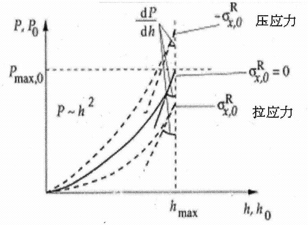
[0045] The stress-free sample film obtained in Example 1 and the film sample without removing the substrate were subjected to a nanoindentation test to obtain the indentation data of the film sample, and then the Suresh theoretical model was used for calculation.
[0046] 1. Using the curvature method to measure the residual stress distribution of the film
[0047] GS6341 electronic thin film stress distribution tester was used to measure the stress distribution of copper film. It uses the principle of laser interference phase shift to measure the change in the radius of curvature of the substrate before and after film formation, and calculates the film stress value according to the Stoney equation.
[0048] σ ( x , y ) = Ed s 2 6 ( 1 - γ ) d f × 1 R ( x , y ) - - - ( 6 )
[0049] Among them: E, γ are the Young's modulus and Poisson's ratio of the NaCl substra...
PUM
 Abstract
Description
Claims
Application Information
 - R&D
- Intellectual Property
- Life Sciences
- Materials
- Tech Scout
- Unparalleled Data Quality
- Higher Quality Content
- 60% Fewer Hallucinations
Browse by: Latest US Patents, China's latest patents, Technical Efficacy Thesaurus, Application Domain, Technology Topic, Popular Technical Reports.
© 2025 PatSnap. All rights reserved.Legal|Privacy policy|Modern Slavery Act Transparency Statement|Sitemap|About US| Contact US: help@patsnap.com


