Manufacturing method of three-layer packaging substrate and three-layer packaging substrate

A technology for packaging substrates and manufacturing methods, which is applied in semiconductor/solid-state device manufacturing, electrical components, electric solid-state devices, etc., and can solve the problems of expensive three-layer substrates, high warpage of three-layer packaging substrates, and asymmetric structure of three-layer substrates and other problems, to achieve the effect of reducing problems, uniform internal stress and increasing thickness

Active Publication Date: 2017-05-24
NAT CENT FOR ADVANCED PACKAGING CO LTD
View PDF5 Cites 0 Cited by
  • Summary
  • Abstract
  • Description
  • Claims
  • Application Information

AI Technical Summary

Problems solved by technology

However, in the three-layer substrate produced in the prior art, due to the different conditions when the adjacent two layers of resin are pressed together, the internal stress between the adjacent two layers of resin is caused. Therefore, the formed three-layer substrate is structurally asymmetrical. Causes the problem of high warpage in the three-layer packaging substrate. In addition, the use of ABF resin to make the three-layer substrate is expensive

Method used


Image

  • Manufacturing method of three-layer packaging substrate and three-layer packaging substrate
  • Manufacturing method of three-layer packaging substrate and three-layer packaging substrate
  • Manufacturing method of three-layer packaging substrate and three-layer packaging substrate

Examples


Embodiment Construction

[0043] The present invention will be further described in detail below in conjunction with the accompanying drawings and embodiments. It should be understood that the specific embodiments described here are only used to explain the present invention, but not to limit the present invention. In addition, it should be noted that, for the convenience of description, only parts related to the present invention are shown in the drawings but not all content.

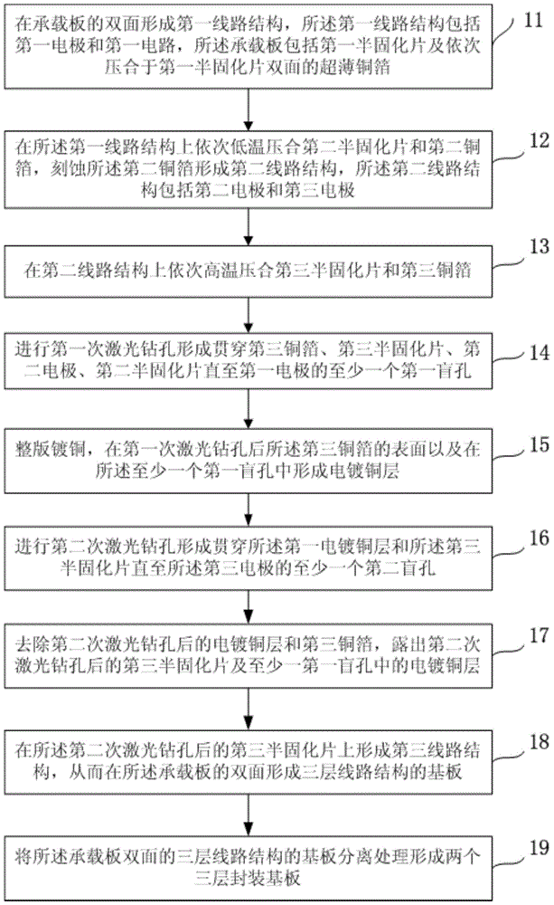
[0044] An embodiment of the present invention provides a method for manufacturing a three-layer packaging substrate. figure 1 It is a flow chart of a method for manufacturing a three-layer packaging substrate according to an embodiment of the present invention, such as figure 1 As shown, the manufacturing method of the three-layer packaging substrate includes:

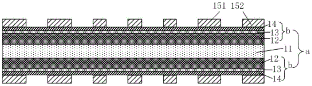
[0045] Step 11, forming a first circuit structure on both sides of the carrier board a, the first circuit structure includes a first electrode 151 and a first circuit...


PUM


Abstract

The invention discloses a manufacturing method of three-layered packaging substrates and three-layered packaging substrates. First circuit structures are formed on both surfaces of a bearing plate, wherein the bearing plate comprises a first half-solidifying slice and ultra-thin copper foils orderly laminated on both faces of the first half-solidifying slice; a second half-solidifying slice and a second copper foil are pressed on the first circuit structures at low temperature, and the second copper foil is etched to form a second circuit structure; a third half-solidifying slice and a third copper foil are pressed on the second circuit structure at high temperature; and then a third circuit structure is formed on the third half-solidifying slice after first laser drilling, full-page copper-coating, second laser drilling and removal of electro-coppering layer; both faces of the bearing plate are formed with the three-layered circuit structural substrates, after separating, solder resist structures are formed on the three-layered circuit structural substrates, thus two three-layered packaging substrates are formed. The manufacturing method of the three-layered packaging substrates and the three-layered packaging substrates can thicken the thickness of an initial structure of the three-layered packaging substrates, and are good for improving yield and avoiding substrate wrapping phenomenon.

Description

technical field [0001] The invention relates to the field of packaging technology, in particular to a method for manufacturing a three-layer packaging substrate and the three-layer packaging substrate. Background technique [0002] With the rapid development of wireless communication, automotive electronics and other consumer electronics, microelectronic packaging technology is developing in the direction of multi-function, miniaturization, portability, high speed, low power consumption and high reliability. Among them, System In a Package (SIP for short) is a new type of packaging technology, which can effectively reduce the packaging area. [0003] The three-layer packaging substrate is a packaging substrate often used in the chip packaging process. The existing three-layer substrate manufacturing method is to use the build-up method to form after the temporary bonding material is coated on both sides of the carrier board and then pressed with ABF resin. For the circuit, ...

Claims


Application Information

Patent Timeline
Patent Type & Authority Patents(China)
IPC IPC(8): H01L21/48H01L23/498H01L21/60
Inventor 于中尧孙瑜张绪
Owner NAT CENT FOR ADVANCED PACKAGING CO LTD
Why Eureka
Try Eureka