Low power consumption fingerprint lock device

A fingerprint lock, low power consumption technology, applied in the direction of electric solid state devices, semiconductor devices, semiconductor/solid state device components, etc., can solve the problem of reducing the height of the module, improve product reliability, enhance data processing speed and power Stable performance, effect of reducing thickness

Active Publication Date: 2017-10-13
苏州科阳半导体有限公司
View PDF4 Cites 0 Cited by
  • Summary
  • Abstract
  • Description
  • Claims
  • Application Information

AI Technical Summary

Problems solved by technology

The Touch ID packaging structure announced by Apple’s patent text is realized by wire bonding, but only grooves are dug on the surface of the chip to reduce the height of the module after wire bonding. I have not seen the packaging form and patent of the fingerprint identification chip that really adopts the wafer-level TSV packaging technology

Method used


Image

  • Low power consumption fingerprint lock device
  • Low power consumption fingerprint lock device
  • Low power consumption fingerprint lock device

Examples


Embodiment 1

[0024] Embodiment 1: A low-power fingerprint lock device, including a fingerprint identification chip 1, a number of blind holes 2 are distributed on the upper surface of the fingerprint identification chip 1, and aluminum pads 3 are arranged in the blind holes 2 of the fingerprint identification chip 1 , the aluminum pad 3 extends from the bottom of the blind hole 2 to the middle of the blind hole 2, and the surface of the aluminum pad 3 in the blind hole 2 is covered with a nickel metal layer 4 and a gold-palladium alloy layer 15 in turn. The middle part extends to the upper surface of the fingerprint identification chip 1 and forms a protrusion to form a pad thickening part 5, and the gold-palladium alloy layer 15 is located on the surface of the pad thickening part 5;

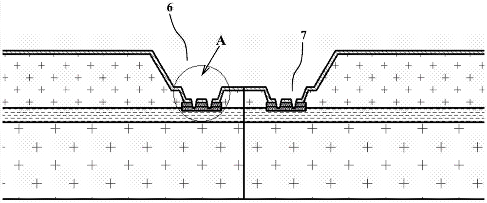
[0025] The lower surface of the fingerprint identification chip 1 and the area opposite to the blind hole 2 have a first tapered blind hole 6 and a second tapered blind hole 7 from outside to inside, and the...

Embodiment 2

[0028] Embodiment 2: A low-power fingerprint lock device, including a fingerprint identification chip 1, a number of blind holes 2 are distributed on the upper surface of the fingerprint identification chip 1, and aluminum pads are arranged in the blind holes 2 of the fingerprint identification chip 1 3. The aluminum pad 3 extends from the bottom of the blind hole 2 to the middle of the blind hole 2, and the surface of the aluminum pad 3 in the blind hole 2 is covered with a nickel metal layer 4 and a gold-palladium alloy layer 15 in sequence. 2. The middle part extends to the upper surface of the fingerprint identification chip 1 and forms a protrusion to form a pad thickening part 5, and the gold-palladium alloy layer 15 is located on the surface of the pad thickening part 5;

[0029] The lower surface of the fingerprint identification chip 1 and the area opposite to the blind hole 2 have a first tapered blind hole 6 and a second tapered blind hole 7 from outside to inside, a...


PUM


Abstract

The invention discloses a fingerprint lock device with low power consumption. There are several blind holes distributed on the upper surface of the fingerprint recognition chip, and aluminum pads are arranged in the blind holes of the fingerprint recognition chip; the lower surface of the fingerprint recognition chip is opposite to the blind holes. The area has a first tapered blind hole and a second tapered blind hole from outside to inside, the second tapered blind hole is located at the bottom of the first tapered blind hole, the first tapered blind hole, the second tapered blind hole The cross-section of the hole is tapered, and the bottom of the second tapered blind hole is the aluminum pad of the fingerprint identification chip. The surface of the aluminum pad in the blind hole is covered with a nickel metal layer and a gold-palladium alloy layer in turn. The nickel metal layer starts from the middle of the blind hole. Extending to the upper surface of the fingerprint recognition chip and forming a bump to form a pad thickening part, the gold-palladium alloy layer is located on the surface of the pad thickening part. The invention overcomes the disadvantage of thick package of the traditional fingerprint identification chip, and realizes low power consumption, small volume and high efficiency integrated fingerprint identification.

Description

technical field [0001] The invention relates to a low-power consumption fingerprint lock device, which belongs to the technical field of semiconductor packaging. Background technique [0002] With the continuous development of mobile communication technology, smart phones have integrated functions in various fields. For example, you can send and receive emails, play video and audio files, record meeting minutes, and even hold video conferences through your smartphone. In addition, a large amount of data is usually stored in a mobile phone used by an individual. If the mobile phone is lost or stolen, it is likely to cause even greater losses. Existing mobile phones are usually protected by digital passwords or graphic passwords, which are cumbersome to store and easily cracked. Therefore, it is popular to use the fingerprint password as the password protection of the mobile phone nowadays, which ensures the security and privacy of the mobile phone. [0003] In terms of ad...

Claims


Application Information

Patent Timeline
Patent Type & Authority Patents(China)
IPC IPC(8): H01L23/488H01L23/31
CPCH01L2224/11
Inventor 黄双武赖芳奇王邦旭吕军刘辰
Owner 苏州科阳半导体有限公司
Why Eureka
Try Eureka