Organic electroluminescence device and manufacturing method for organic electroluminescence device
An electroluminescent device and electroluminescent technology, applied in the direction of electric solid device, semiconductor/solid state device manufacturing, electrical components, etc., can solve the problems of refractive index difference, total reflection loss, low light output performance, etc., and achieve long life and attenuation. The effect of reducing the speed and increasing the transfer rate
- Summary
- Abstract
- Description
- Claims
- Application Information
AI Technical Summary
Problems solved by technology
Method used
Image


Examples
preparation example Construction
[0037] The preparation method of the organic electroluminescence device 100 of an embodiment, it comprises the following steps:
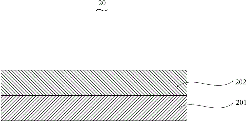
[0038] Step S110 , preparing the scattering layer 20 on the surface of the glass substrate 10 by electron beam evaporation.
[0039] The scattering layer 20 is formed on one side surface of the glass substrate 10 . The scattering layer 20 is composed of a metal material layer 201 and a ternary doped layer 202. The metal material layer 201 is prepared on the surface of the glass substrate 10 by thermal resistance evaporation, and the work function of the metal material is -4.0eV~-5.5eV. A ternary doped layer 202 is prepared on the surface of the metal material layer 201 by thermal resistance evaporation, and the ternary doped layer 202 includes a lithium salt material, a luminescent material and a hole guest material, and the luminescent material is selected from 4- (Dinitrile methyl)-2-butyl-6-(1,1,7,7-tetramethyljulonesidine-9-vinyl)-4H-pyran (DCJ...
Embodiment 1
[0059] The structure prepared in this example is glass substrate / Ag / Li 2 O:Alq 3 :F4-TCNQ / ITO / MoO 3 / NPB / Alq 3 / TAZ / CsF / Ag organic electroluminescent device, in this embodiment and the following embodiments, " / " indicates a layer, and ":" indicates doping.
[0060] The glass substrate is N-LASF44. After rinsing the glass substrate with distilled water and ethanol, soak it in isopropanol for one night. Prepare the scattering layer on the glass substrate. The scattering layer is composed of a metal material layer and a ternary doped layer. The metal material layer is prepared by thermal resistance evaporation on the surface of the glass substrate. The material is Ag and the thickness is 30nm. The ternary doped layer was prepared by thermal resistance evaporation, and the material was Li 2 O:Alq 3 :F4-TCNQ,Li 2 O, Alq 3 The mass ratio to F4-TCNQ is 6:5:0.1, and the thickness is 100nm. Then ITO is prepared on the scattering layer with a thickness of 100nm, which is prepare...
Embodiment 2
[0067] The structure prepared in this example is glass substrate / Al / LiF:DCJTB:1T-NATA / AZO / V 2 o 5 / TAPC / ADN / Bphen / CsN 3 / Al organic electroluminescent devices.
[0068] The glass substrate is N-LAF36. After rinsing the glass substrate with distilled water and ethanol, soak it in isopropanol for one night to prepare a scattering layer on the glass substrate. The scattering layer is composed of a metal material layer and a ternary doped layer. The metal material layer is prepared by thermal resistance evaporation on the surface of the glass substrate, the material is Al, and the thickness is 20nm, and the ternary doped layer is prepared by thermal resistance evaporation on the surface of the metal material layer, and the material is LiF:DCJTB:1T-NATA, LiF: DCJTB: 1T-NATA. The mass ratio is 3:2:0.1, and the thickness is 200nm. Then AZO is prepared on the scattering layer with a thickness of 80nm, which is prepared by magnetron sputtering; the hole injection layer is evaporate...
PUM
 Abstract
Description
Claims
Application Information
 - R&D
- Intellectual Property
- Life Sciences
- Materials
- Tech Scout
- Unparalleled Data Quality
- Higher Quality Content
- 60% Fewer Hallucinations
Browse by: Latest US Patents, China's latest patents, Technical Efficacy Thesaurus, Application Domain, Technology Topic, Popular Technical Reports.
© 2025 PatSnap. All rights reserved.Legal|Privacy policy|Modern Slavery Act Transparency Statement|Sitemap|About US| Contact US: help@patsnap.com