
Method for improving light emitting property of LED by using laser radiated gallium nitride epitaxial wafer as substrate of LED

A technology of luminescence performance and laser irradiation, which is applied in the direction of electrical components, circuits, semiconductor devices, etc., can solve problems such as the late start of research on luminescent materials for blue LEDs, and the material performance has not reached the level expected by people, and achieves laser irradiation parameters. Accurate and controllable, significantly improved electro-optical properties, and short time period

Active Publication Date: 2015-05-27
BEIJING UNIV OF TECH
View PDF1 Cites 4 Cited by
  • Summary
  • Abstract
  • Description
  • Claims
  • Application Information

AI Technical Summary

Problems solved by technology

At present, how to improve the luminous performance of GaN-based blue LEDs is one of the global academic hotspots. The reason is that the research on the luminescent materials of blue LEDs started late, and its material properties have not reached the expected level.

Method used


Image

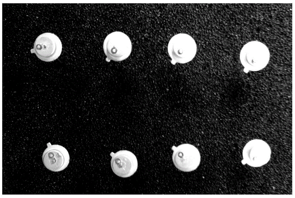
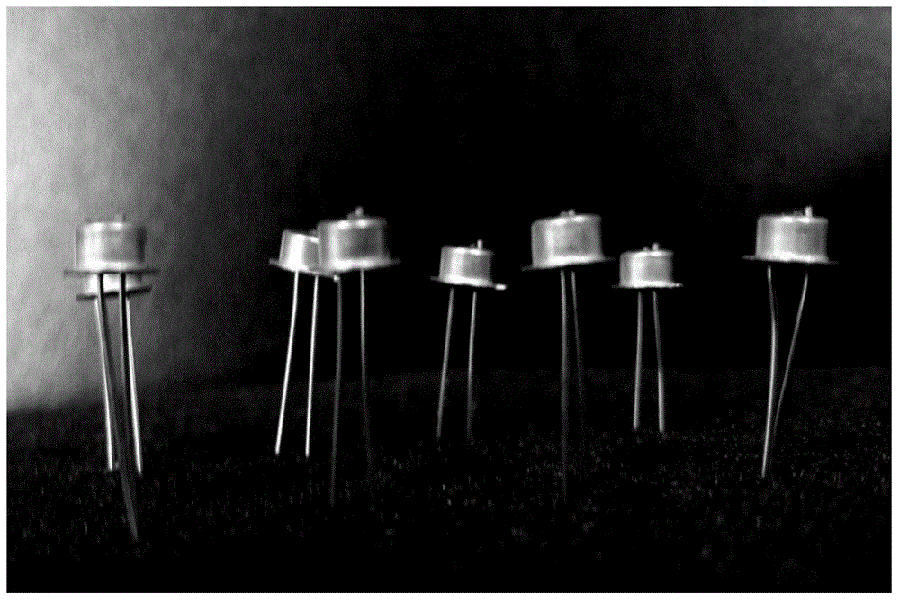
  • Method for improving light emitting property of LED by using laser radiated gallium nitride epitaxial wafer as substrate of LED
  • Method for improving light emitting property of LED by using laser radiated gallium nitride epitaxial wafer as substrate of LED
  • Method for improving light emitting property of LED by using laser radiated gallium nitride epitaxial wafer as substrate of LED

Examples


Embodiment 1

[0028] Cut the gallium nitride epitaxial wafer into square samples with a size of about 1cm×1cm each with a glass knife; immerse in acetone solvent for ultrasonic cleaning for 5 minutes, then rinse; immerse in alcohol solvent for ultrasonic cleaning for 5 minutes, then rinse; immerse in deionized water After ultrasonic cleaning for 10 min, rinse and dry. Put the pretreated gallium nitride epitaxial wafer on the target stage, and irradiate it with an excimer laser with a wavelength of 248nm in air, oxygen, and nitrogen environments (the air pressure is a standard atmospheric pressure); the pulse laser frequency 3Hz, single pulse energy density 0.5J / cm 2 , the number of pulses is 90. The out-of-focus amount is 4cm, and the compound eye structure is used to shape the outgoing laser light, and the spot area acting on the sample is 1cm 2, that is, a square spot with a size of 1cm×1cm. The samples obtained before and after irradiation were all deposited Ni (30nm) / Au (100nm) metal...

Embodiment 2

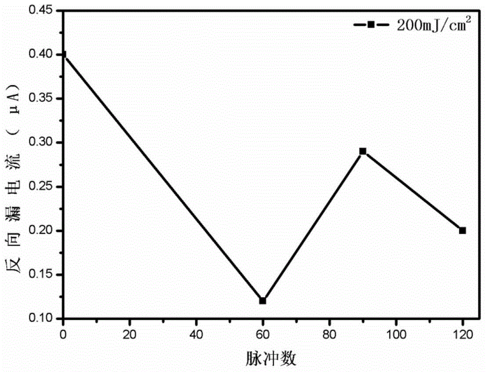
[0031] Cut the gallium nitride epitaxial wafer into square samples with a size of about 1cm×1cm each with a glass knife; immerse in acetone solvent for ultrasonic cleaning for 5 minutes, then rinse; immerse in alcohol solvent for ultrasonic cleaning for 5 minutes, then rinse; immerse in deionized water After ultrasonic cleaning for 10 min, rinse and dry. Place the pretreated GaN epitaxial wafer on the target stage, and irradiate it with an excimer laser with a wavelength of 248nm in an atmospheric environment; the pulse laser frequency is 3Hz, and the single pulse energy density is 0.2-0.6J / cm 2 , the number of pulses is 60, 90, 120. The out-of-focus amount is 4cm, and the compound eye structure is used to shape the outgoing laser light, and the spot area acting on the sample is 1cm 2 , that is, a square spot with a size of 1cm×1cm. After cleaning, evaporating ITO, step (mesa) lithography, ICP etching, glue removal, ITO alloy, HF acid cleaning, patterned pad lithography sp...


PUM


Abstract

The invention discloses a method for improving the light emitting property of an LED by using a laser radiated gallium nitride epitaxial wafer as the substrate of the LED, and belongs to the field of material preparation. The method comprises the following steps: firstly, pretreating the GaN epitaxial wafer (the surface of the epitaxial wafer is of a p type) so as to remove pollution attachment, organic residues and the like on the surface and reducing the lattice imperfection of the surface; radiating the GaN epitaxial wafer by using a 248nm excimer laser with the single pulse energy density of 0.15J / cm<2> to 0.6J / cm<2>, depositing a metal electrode on the surface of a sample according to a magnetron sputtering method, and further performing electric testing on metal semiconductor ohmic contact such as the carrier concentration and the surface resistivity, the testing result shows that various electric properties of the radiated sample are remarkably changed, and thus the ohmic contact of the radiated sample is greatly improved. The GaN epitaxial wafer before or after being radiated is manufactured by using a progress LED process, the LED characteristic parameters such as the positive voltage, the negative leakage current and the light emission power of the LED are tested, and the result shows that the LED characteristic parameters are all improved to different extents.

Description

technical field [0001] The invention belongs to the field of material preparation. Background technique [0002] Wide bandgap semiconductors represented by materials such as gallium nitride and silicon carbide are emerging materials with rich physical properties, and many of their electrical and optical properties far exceed those of the previous generation of semiconductor materials. Wide bandgap semiconductors are playing an increasingly important role in current production and life, especially gallium nitride materials play a pivotal role in the human lighting industry, and are widely used in the new generation of lighting LED devices. [0003] The bandgap of GaN material is direct bandgap type, and its bandgap width is 3.39eV at room temperature, which belongs to the category of wide bandgap semiconductors, and generally has a high quantum efficiency during carrier recombination. The GaN material has a direct band gap, which means that it has a wide band gap, and is ver...

Claims


Application Information

Patent Timeline
Patent Type & Authority Applications(China)
IPC IPC(8): H01L33/32H01L33/00
CPCH01L21/02002H01L21/322H01L33/00H01L33/32
Inventor 蒋毅坚谈浩琪赵艳
Owner BEIJING UNIV OF TECH
Learn More