


Quick Research
Generate reliable direction feasibility study reports for your R&D in just a few steps.

Technical Q&A
Discover and master advanced knowledge NOW. Basics, ideas, possibilities, all at once.

Find Solutions
As an expert in R&D theories, this can generate solutions to your technical problems instantly.

Evaluate Feasibility
Analyze your overall solution with one click, know your potential R&D risks in advance.

Monitor Landscape
Get weekly tech updates, stay abreast of the latest tech innovations and key insights.
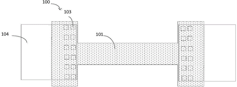
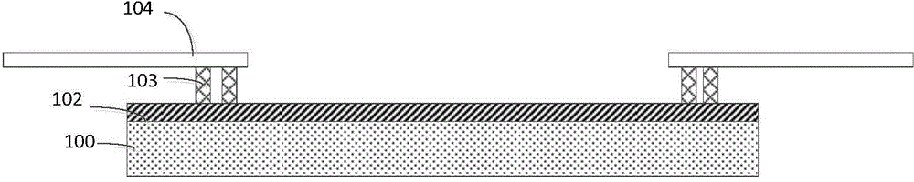
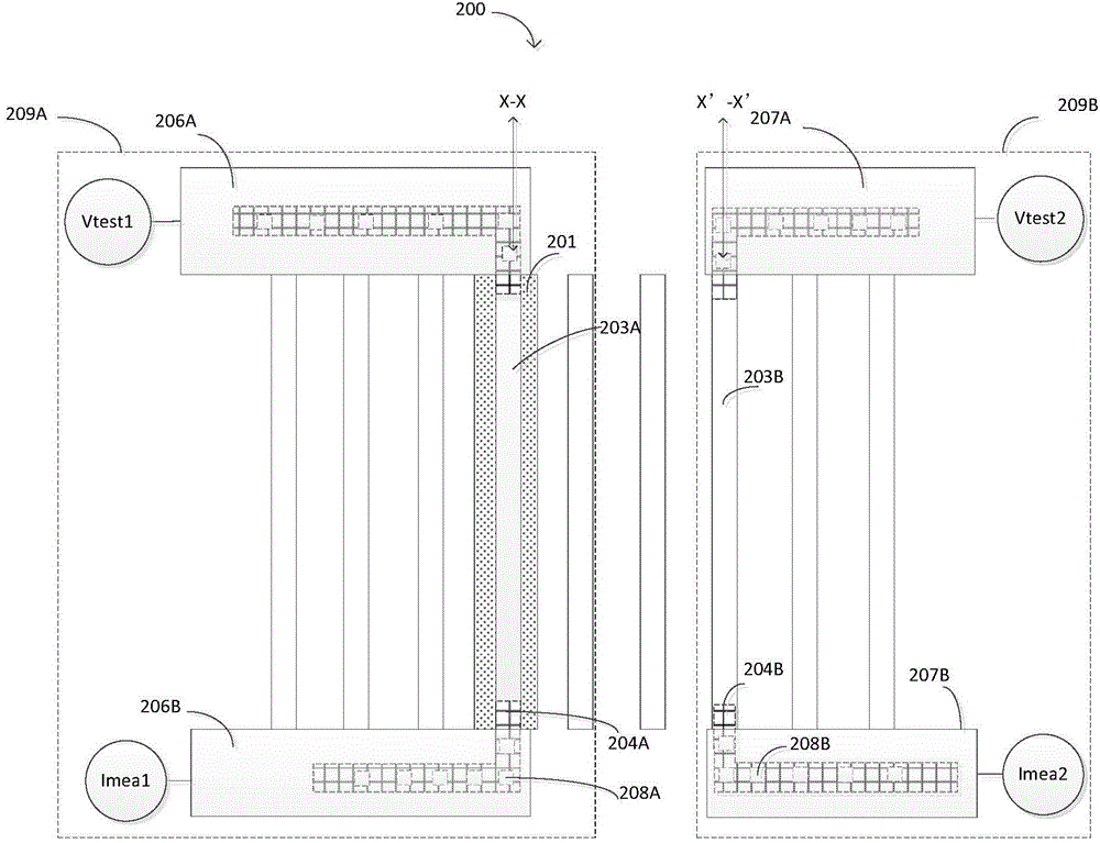
Test structure used for measuring silicide resistance
A technology for testing structures and silicides, which is used in semiconductor/solid-state device testing/measurement, circuits, electrical components, etc., to solve problems such as inability to use silicide resistance measurement, and achieve accurate measurement results.
- Summary
- Abstract
- Description
- Claims
- Application Information
AI Technical Summary
Problems solved by technology
Method used
Image

Examples
Embodiment Construction
[0025] In the following description, a lot of specific details are given in order to provide a more thorough understanding of the present invention. However, it is obvious to those skilled in the art that the present invention can be implemented without one or more of these details. In other examples, in order to avoid confusion with the present invention, some technical features known in the art are not described. In order to thoroughly understand the present invention, a detailed description will be provided in the following description to illustrate the method of the present invention. Obviously, the implementation of the present invention is not limited to the specific details familiar to those skilled in the semiconductor field. The preferred embodiments of the present invention are described in detail as follows. However, in addition to these detailed descriptions, the present invention may also have other embodiments.
[0026] It should be noted that the terms used here ...
PUM
 Abstract
Description
Claims
Application Information
 - R&D Engineer
- R&D Manager
- IP Professional
- Industry Leading Data Capabilities
- Powerful AI technology
- Patent DNA Extraction
Browse by: Latest US Patents, China's latest patents, Technical Efficacy Thesaurus, Application Domain, Technology Topic, Popular Technical Reports.
© 2024 PatSnap. All rights reserved.Legal|Privacy policy|Modern Slavery Act Transparency Statement|Sitemap|About US| Contact US: help@patsnap.com