
Composition used for cleaning after chemical mechanical polishing

A technology of chemical machinery and composition, applied in the direction of detergent composition, organic non-surface active detergent composition, non-surface active detergent composition, etc., can solve the problems of semiconductor quality reduction, equipment reliability reduction, corrosion, etc. Achieve the effect of excellent semiconductor

Active Publication Date: 2015-05-20
DONGJIN SEMICHEM CO LTD
View PDF3 Cites 0 Cited by
  • Summary
  • Abstract
  • Description
  • Claims
  • Application Information

AI Technical Summary

Problems solved by technology

[0005] However, since unexpected substances are deposited on the surface of the liquid crystal panel after cleaning, the quality of the manufactured semiconductor is reduced, and the cleaning liquid comes into contact with the exposed copper wiring, causing wedges along the interface between metal films such as Ta and TaN and copper wiring. Form corrosion, which may reduce the reliability of the equipment, the so-called side seam phenomenon

Method used


Image

  • Composition used for cleaning after chemical mechanical polishing
  • Composition used for cleaning after chemical mechanical polishing

Examples


Embodiment 1 to 3 and comparative example 1 to 7

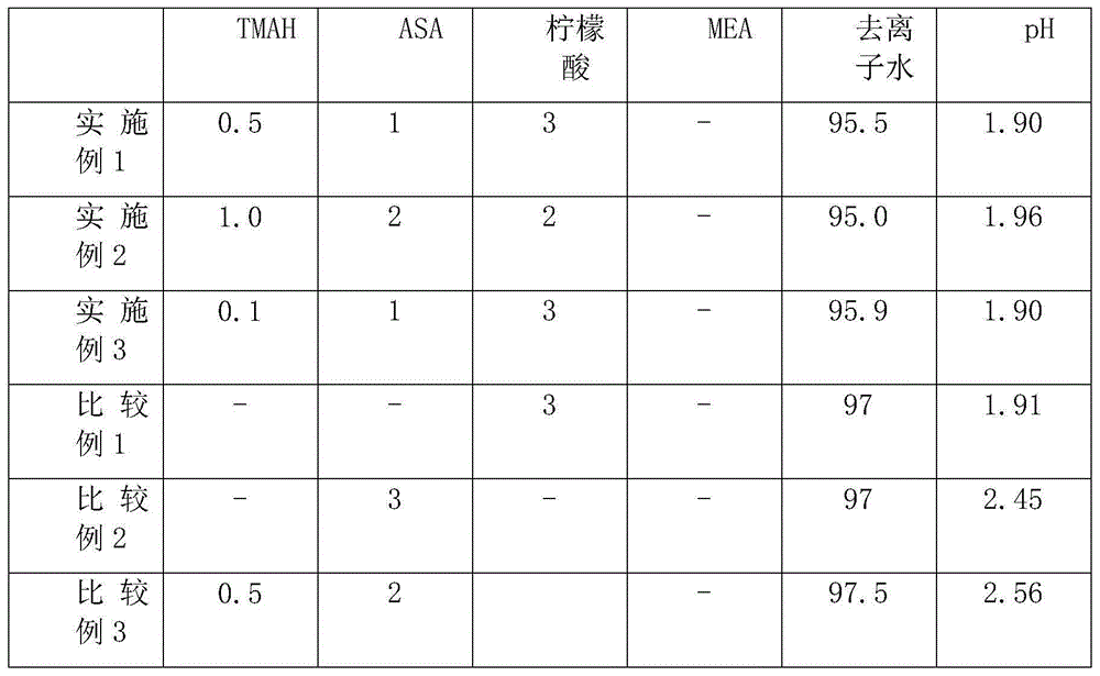
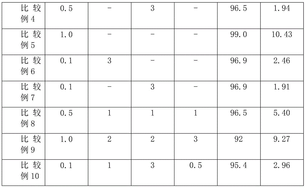
[0040] The composition of Table 1 below was prepared by mixing tetramethylammonium hydroxide (TMAH), ascorbic acid (ASA), citric acid, monoalcohol amine (MEA) as an amine compound other than TMAH, and deionized water. Compositions for cleaning after chemical mechanical polishing. (unit weight%)

[0041] [Table 1]

[0042]

[0043]

[0044]

[0045] Cleaning power evaluation test

[0046] After depositing 5.5KA thermal oxide layer (Thermal Oxide), 250A tantalum (Ta), and 1KA copper seed layer (Cu seed) on the silicon Si wafer, electroplating (Electro-Platating, EP) on 15KA copper (Cu), thus making A wafer with exposed metal components on the surface. The fabricated wafer is put into a CMP device and subjected to chemical mechanical polishing with a polishing slurry comprising Planar solution, hydrogen peroxide and distilled water.

[0047] After chemical mechanical polishing, put the chemical mechanically polished wafer into the On track device, and spray it with ...


PUM


Abstract

The invention relates to a composition used for cleaning after chemical mechanical polishing, to be specific, relates to the cleaning technology used for the semiconductor substrate having the metal wiring and the metal film in the semiconductor production technology, and especially relates to the composition used for cleaning the semiconductor substrate having the exposed metal wiring after the chemical mechanical polishing. The cleaning composition can be used to clean the impurities of the semiconductor work pieces effectively without damaging the metal wiring, and after the cleaning, the work piece pollution of the surface can be prevented, and therefore the good semiconductor can be produced.

Description

technical field [0001] The present invention relates to a kind of composition that is used for cleaning after chemical mechanical polishing (post CMP), more particularly, relates to a kind of in semiconductor manufacturing process, is used for the cleaning process of the semiconductor substrate that comprises metal wiring and metal film, especially Composition for cleaning semiconductor substrates with exposed metal wiring after chemical mechanical polishing. Background technique [0002] With miniaturization of semiconductor devices and multilayer wiring structures, a method capable of more precisely planarizing the surface of a substrate is required at each stage of the semiconductor manufacturing process. In particular, when using multilayer metals such as copper deposited on a silicon substrate for connection to the active area of ​​a silicon wafer, the following steps are performed: Copper is deposited in lines etched in an interlayer dielectric by a damascene process, ...

Claims


Application Information

Patent Timeline
Patent Type & Authority Applications(China)
IPC IPC(8): C11D7/32C11D7/26C11D7/60
CPCC11D7/26C11D7/32H01L21/306C11D2111/22
Inventor 张斗瑛金炳郁赵泰杓尹锡壹许舜范韩莹圭
Owner DONGJIN SEMICHEM CO LTD
Learn More