Low-temperature polycrystalline silicon thin film transistor, manufacturing method, array substrate and display device

A low-temperature polysilicon and thin-film transistor technology, which is used in transistors, semiconductor/solid-state device manufacturing, semiconductor devices, etc., can solve the problems of thin-film transistors such as poor threshold voltage uniformity, uneven ion implantation depth, and inability to realize source-drain ultra-shallow junctions. , to achieve good depth uniformity, reduce channel effect, and good uniformity

Active Publication Date: 2015-05-13
BOE TECH GRP CO LTD
View PDF6 Cites 4 Cited by
  • Summary
  • Abstract
  • Description
  • Claims
  • Application Information

AI Technical Summary

Problems solved by technology

[0004] In the current manufacturing process of low-temperature polysilicon thin film transistors, one of the steps is to form a layer of polysilicon thin film on the substrate, and the subsequent process will form the source / drain region and channel region of the thin film transistor based on the polysilicon thin film. In order to improve the thin film transistor performance, it is necessary to perform ion implantation on the polysilicon film in the source / drain region, such as figure 1 and figure 2 As shown, when ion implantation is performed on polysilicon thin films, ions are directly implanted on the surface of polysilicon thin films. Since the arrangement of lattice atoms in polysilicon is regular, there will be a channeling effect, resulting in uneven depth of ion implantation, which in turn causes thin film The uniformity of the threshold voltage (Vth) of the transistor is poor, and the source-drain ultra-shallow junction cannot be realized

Method used


Image

  • Low-temperature polycrystalline silicon thin film transistor, manufacturing method, array substrate and display device
  • Low-temperature polycrystalline silicon thin film transistor, manufacturing method, array substrate and display device
  • Low-temperature polycrystalline silicon thin film transistor, manufacturing method, array substrate and display device

Examples


Embodiment 1

[0036] This embodiment provides a method for manufacturing a low-temperature polysilicon thin film transistor, including:

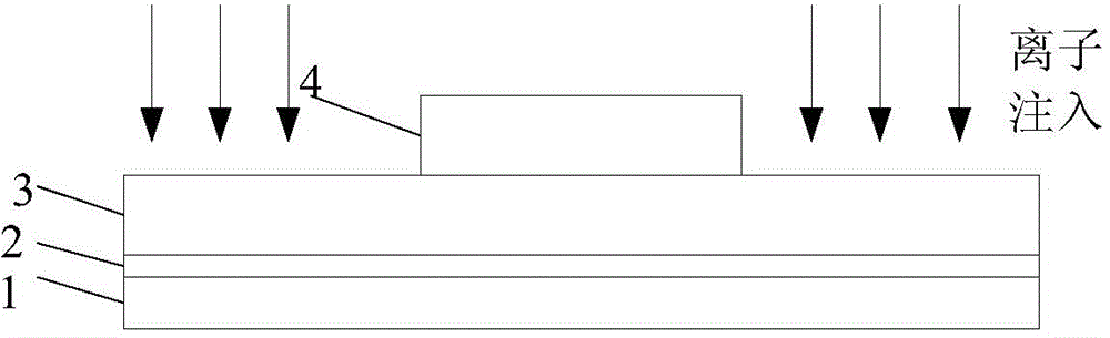
[0037] Forming an active layer comprising a source region and a drain region by using a low-temperature polysilicon film, the source region is used to contact the source electrode of the thin film transistor, and the drain region is used to contact the drain electrode of the thin film transistor;

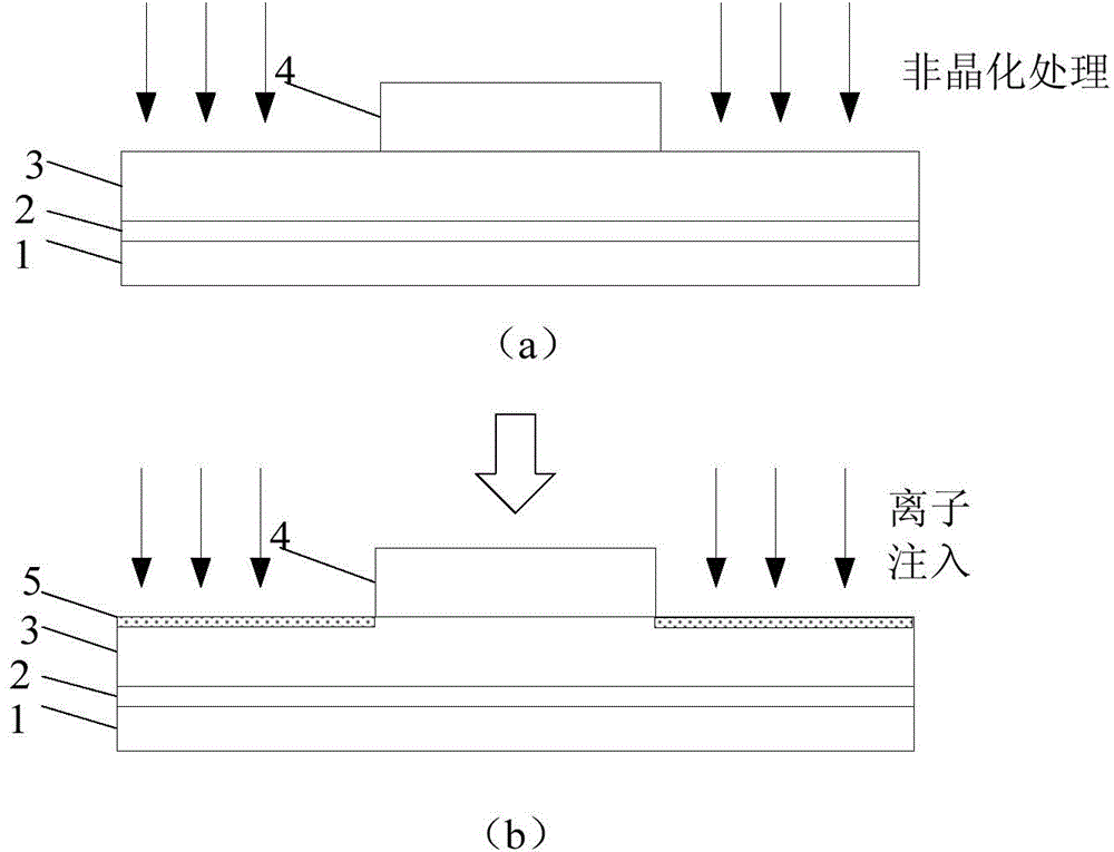
[0038] forming an amorphous silicon layer on the surface of the low-temperature polysilicon film in the source region and the drain region;

[0039] Ion implantation is performed on the low-temperature polysilicon film on which the amorphous silicon layer is formed on the surface.

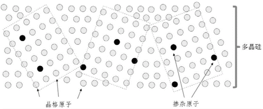
[0040] In this embodiment, an amorphous silicon layer is formed on the surface of the low-temperature polysilicon film before ion implantation is performed on the low-temperature polysilicon film in the source region and the drain region. Since the lattice atoms in the amorphous sil...

Embodiment 2

[0050] This embodiment also provides a low-temperature polysilicon thin film transistor, which is manufactured by the above-mentioned method.

[0051] In the low-temperature polysilicon thin film transistor of this embodiment, the ion implantation depth uniformity of the source region / drain region of the active layer is better, the threshold voltage uniformity of the thin film transistor is better, and the source-drain ultra-shallow junction can be realized.

Embodiment 3

[0053] An embodiment of the present invention also provides an array substrate, including the above-mentioned low temperature polysilicon thin film transistor formed on the base substrate.


PUM


Abstract

The invention provides a low-temperature polycrystalline silicon thin film transistor, a manufacturing method, an array substrate and a display device, and belongs to the technical field of displaying. The manufacturing method comprises the steps of: using low-temperature polycrystalline silicon thin film forming the active layer includes a source region and a drain region, said source region for contact with the source electrode of the thin film transistor, said drain region for contact with the drain electrode of the thin film transistor; the source low-temperature polysilicon thin film surface region and a drain region forming an amorphous silicon layer; the surface of the low-temperature polycrystalline silicon thin film formed on the amorphous silicon layer by ion implantation. The transistor can reduce the channel effect, so that the depth of ion implantation uniformity better uniformity of the threshold voltage of the thin film transistor is preferably, and to achieve ultra-shallow source and drain junctions.

Description

technical field [0001] The invention relates to the field of display technology, in particular to a low-temperature polysilicon thin film transistor, a manufacturing method, an array substrate and a display device. Background technique [0002] Organic light-emitting display (OLED) has attracted much attention due to its many advantages such as self-illumination, fast response, thinness, low power consumption and flexible display, and is considered to be the next generation of flat panel display technology. At present, OLED technology has been gradually applied to various electronic products, among which the active matrix organic light-emitting display (AMOLED) is famous for its advantages of high image quality, short response time of moving images, low power consumption, wide viewing angle and ultra-light and ultra-thin. Become the main trend of OLED development. [0003] At present, polysilicon thin film transistors are mostly used in AMOLED backplane technology, and poly...

Claims


Application Information

Patent Timeline
Patent Type & Authority Applications(China)
IPC IPC(8): H01L29/786H01L21/336H01L21/266
CPCH01L21/26506H01L21/266H01L29/6675H01L29/78672
Inventor 陆小勇刘政李小龙田慧孙亮王祖强
Owner BOE TECH GRP CO LTD
Why Eureka
Try Eureka