Substrate, manufacturing method thereof and display device
A substrate and group technology, applied in the field of semiconductor display, can solve problems such as over-cutting, unsatisfactory results, affecting TFT characteristics, etc., and achieve the effect of preventing peeling
- Summary
- Abstract
- Description
- Claims
- Application Information
AI Technical Summary
Problems solved by technology
Method used
Image
Examples
Embodiment 1
[0068] This embodiment provides a substrate with copper electrodes as gates.
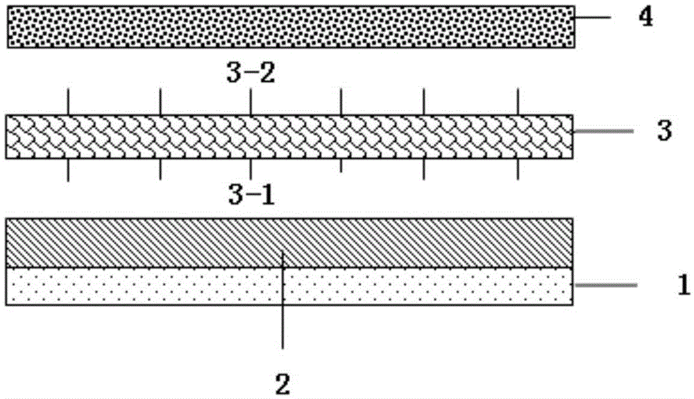
[0069] Such as figure 2 As shown, the substrate described in this embodiment includes a substrate 1, and a gate 2 and a photoresist layer 4 (positive photoresist) formed on the substrate 1. Meanwhile, the gate 2 and the photoresist layer A copper diffusion / photoresist peeling improvement layer 3 is also formed between the 4.
[0070] Wherein, the gate 2 is a copper single-layer structure, and the copper diffusion / photoresist peeling improvement layer 3 is formed by depositing mercaptoundecanoic acid (MUA) on the gate as a material, and is deposited on the copper metal by a spin coating method with a thickness of 20nm mercapto undecanoic acid, molecular surface group 3-1 (in this embodiment is -SH group) contacts with copper, is used to prevent copper from diffusing; Molecular chain end group 3-2 (in this embodiment is -COOH group) is in contact with the positive photoresist to prevent the photore...
Embodiment 2
[0072] Compared with Embodiment 1, the only difference is that in this embodiment, the gate 2 (copper electrode) is a double-layer structure composed of a single layer of copper and a diffusion barrier layer, wherein the single layer of copper is the The top layer of the diffusion / photoresist stripping improvement layer contact, the diffusion prevention layer is formed of polyethyleneimine (PEI) material, specifically adopting the thermal evaporation method to deposit polyethyleneimine with a thickness of 50nm on the bottom of the single layer of copper, wherein, Molecular surface group - COO - It is in contact with copper to prevent copper diffusion; the end group of the molecular chain is -OH, which is in contact with the substrate to prevent the substrate from falling off.
Embodiment 3
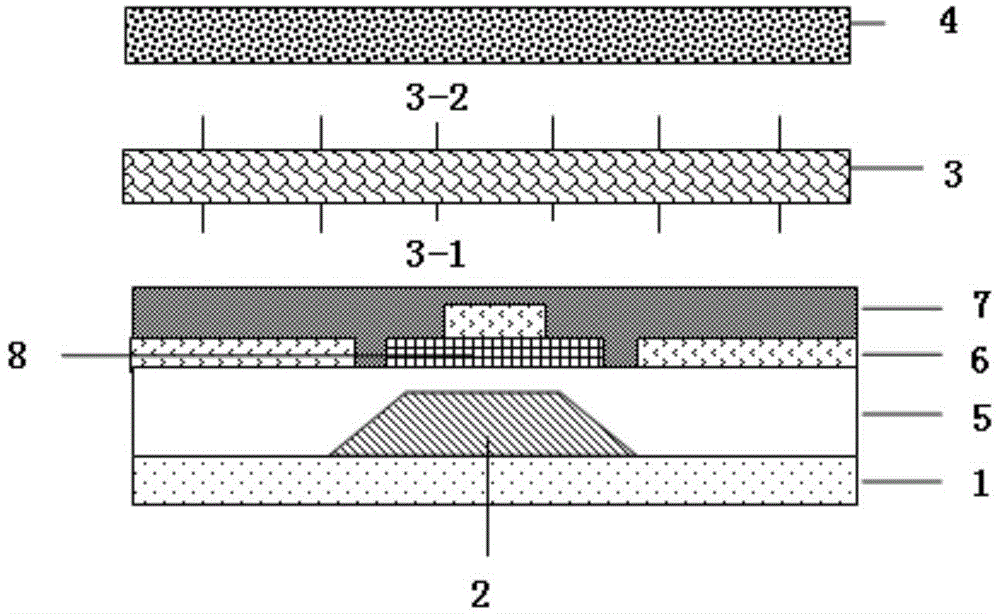
[0074] Compared with Embodiment 1, the only difference is that in this embodiment, the gate 2 is a double-layer structure composed of a single layer of copper and a diffusion preventing layer.
[0075] Wherein the diffusion / photoresist peeling improvement layer located above the single layer copper is formed on the gate 2 by spin-coating method of mercaptoundecanoic acid material, with a thickness of 5nm; the molecular surface group -SH of mercaptoundecanoic acid and copper Contact to prevent metal copper from diffusing, and the molecular chain end group -COOH of mercaptoundecanoic acid contacts with positive photoresist to prevent photoresist from falling off. The diffusion barrier layer constituting a part of the gate 2 is formed of polyethyleneimine material, and polyethyleneimine is deposited on the bottom of the single-layer copper by thermal evaporation method, with a thickness of 10nm. The molecular surface group of polyethyleneimine-COO - It is in contact with copper t...
PUM
| Property | Measurement | Unit |
|---|---|---|
| thickness | aaaaa | aaaaa |
| thickness | aaaaa | aaaaa |
| thickness | aaaaa | aaaaa |
Abstract
Description
Claims
Application Information
 - Generate Ideas
- Intellectual Property
- Life Sciences
- Materials
- Tech Scout
- Unparalleled Data Quality
- Higher Quality Content
- 60% Fewer Hallucinations
Browse by: Latest US Patents, China's latest patents, Technical Efficacy Thesaurus, Application Domain, Technology Topic, Popular Technical Reports.
© 2025 PatSnap. All rights reserved.Legal|Privacy policy|Modern Slavery Act Transparency Statement|Sitemap|About US| Contact US: help@patsnap.com


