Semiconductor structure and forming method thereof

A technology of semiconductor and gate structure, applied in the field of semiconductor structure and its formation, can solve the problems of improvement and limited improvement of parasitic capacitance, etc.

Active Publication Date: 2015-05-13
SEMICON MFG INT (SHANGHAI) CORP
View PDF5 Cites 9 Cited by
  • Summary
  • Abstract
  • Description
  • Claims
  • Application Information

AI Technical Summary

Problems solved by technology

[0005] With the reduction of the spacing between the gate structures, the difficulty of forming low-K sidewalls on both sides of the gate in the prior art is also gradually increasing, and the improvement effect of the parasitic capacitance by the method of the prior art is limited, and the performance of the transistor is still low. To be further improved

Method used


Image

  • Semiconductor structure and forming method thereof
  • Semiconductor structure and forming method thereof
  • Semiconductor structure and forming method thereof

Examples


Embodiment Construction

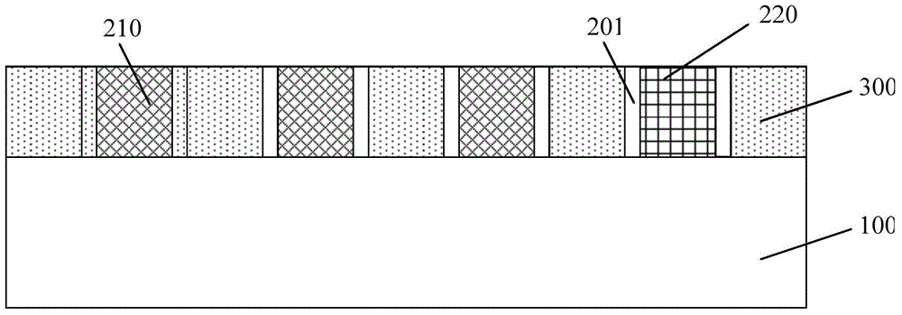
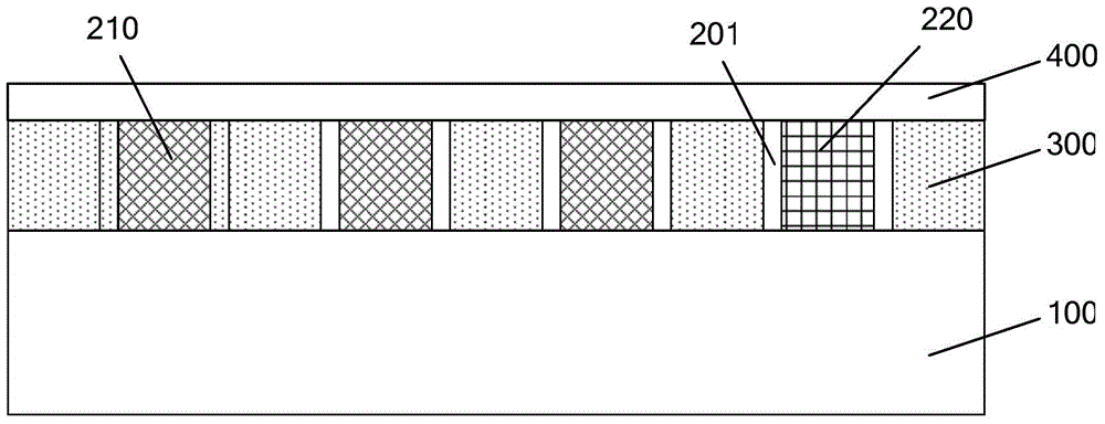
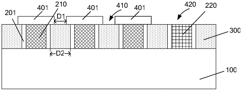
[0031] As mentioned in the background, there is high parasitic capacitance between the gates of transistors in the prior art, which affects the performance of transistors and circuits.

[0032] Although the existing technology can reduce the parasitic capacitance between adjacent gates by using low-K materials to form sidewalls on both sides of the gate, but due to the poor adhesion between the low-K material and the gate, the gate The quality of the sidewall formed on the sidewall surface is poor, and, as the process node continues to shrink, the difficulty of forming a sidewall of low-K material on the sidewall of the gate is further increased, thereby affecting the parasitic capacitance between the gates of the transistor The improvement effect is limited.

[0033] In the embodiment of the present invention, the parasitic capacitance between the gate structures is reduced by forming an air gap in the dielectric layer between the adjacent gate structures, thereby improving t...


PUM


Abstract

The invention provides a semiconductor structure and a forming method thereof. The forming method of the semiconductor structure comprises the steps of providing a semiconductor substrate, forming an insulating layer for covering a sacrificial layer and a plurality of first gate structures, etching the insulating layer, and forming a first opening in the surface of the sacrificial layer between the adjacent first gate structures to expose partial surface of the sacrificial layer between the adjacent first gate structures, removing the sacrificial layer, and forming a dielectric layer on the surface of the semiconductor substrate, wherein the plurality of first gate structures, and the sacrificial layer located on the surface of the semiconductor substrate and flush with the surface of the first gate structure are formed on the surface of the semiconductor substrate; the surface of the dielectric layer is higher than that of the insulating layer, and an air gap is formed in the dielectric layer between the adjacent first gate structures. According to the semiconductor device formed by the method, the parasitic capacitance between the adjacent gate structures can be reduced and the performance of a semiconductor device can be improved.

Description

technical field [0001] The invention relates to the technical field of semiconductors, in particular to a semiconductor structure and a forming method thereof. Background technique [0002] As the integration level of integrated circuits becomes higher and higher, the technology nodes of semiconductor processes become smaller and smaller, so that the distance between adjacent devices becomes smaller and smaller. On the same chip, the distance between the gates of different transistors is getting smaller and smaller, which will lead to larger and larger parasitic capacitance values ​​between adjacent gates, and the parasitic capacitance will cause capacitive coupling between the gates Rise, thereby increasing energy consumption and increasing the resistance-capacitance (RC) time constant, affecting the running speed of the chip, and also having a serious impact on the reliability of the devices on the chip. [0003] For example, for a fin field effect transistor with a high-...

Claims


Application Information

Patent Timeline
Patent Type & Authority Applications(China)
IPC IPC(8): H01L27/04H01L21/77
Inventor 三重野文健
Owner SEMICON MFG INT (SHANGHAI) CORP
Why Eureka
Try Eureka