Wafer Level Packaging Method

A wafer-level packaging and substrate technology, applied in the manufacturing of electrical components, circuits, semiconductor/solid-state devices, etc., can solve problems such as unevenness, damage to the TSV and the back of the substrate, affecting the electrical signal of the TSV metal layer, etc. , to achieve the effect of good performance and good electrical signal

Active Publication Date: 2018-09-14
SEMICON MFG INT (SHANGHAI) CORP +1
View PDF9 Cites 0 Cited by
  • Summary
  • Abstract
  • Description
  • Claims
  • Application Information

AI Technical Summary

Problems solved by technology

[0009] The problem to be solved by the present invention is that, using the wafer-level packaging method based on TSV technology in the prior art, the TSV and the back of the substrate are damaged and uneven, which affects the electrical signal of the metal layer in the TSV, resulting in packaging Poor performance of the structure

Method used


Image

  • Wafer Level Packaging Method
  • Wafer Level Packaging Method
  • Wafer Level Packaging Method

Examples


Embodiment Construction

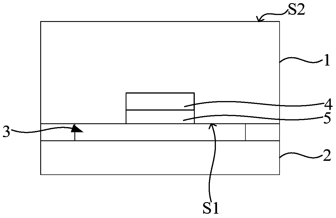
[0043] Aiming at the problems existing in the prior art, this technical solution proposes a new wafer-level packaging method. Using this wafer-level packaging method, after the first through hole is formed in the substrate, a relatively thin polymer layer is firstly formed on the back side of the substrate and the sidewall of the first through hole, and the polymer layer serves as the back side of the substrate and the sidewall of the first through hole. A protection layer for the sidewall of the through hole; then, etching the interlayer dielectric layer, and simultaneously etching and removing the polymer layer. Afterwards, the process of forming the polymer layer and etching the interlayer dielectric layer is repeated until the pad is exposed, and a second through hole is formed, and the second through hole is used as a silicon through hole.

[0044] In order to make the above objects, features and advantages of the present invention more comprehensible, specific embodiment...


PUM


Abstract

The invention discloses a wafer level packaging method. The wafer level packaging method includes that providing a substrate, wherein the substrate has a front surface and a back surface, and an interlevel dielectric layer and a welding pad located on the interlevel dielectric layer are formed in the front surface; forming a first through hole in the back of the substrate, wherein the interlevel dielectric layer exposes out of the first through hole; forming a polymer layer at each of the back surface of the substrate and the side wall of the first through hole; etching the interlevel dielectric layer, and etching to remove the polymer layers when etching the interlevel dielectric layer; repeating the steps of forming the polymer layer at each of the back surface of the substrate and the side wall of the first through hole, etching the interlevel dielectric layer, and etching to remove the polymer layers when etching the interlevel dielectric layer till exposing the welding pad, and forming a second through hole. According to the technical scheme, when etching the interlevel dielectric layer, the polymer layers protect the back of the substrate and the side wall of the first through hole from damage, the surfaces of the back of the substrate and the side wall of the first through hole are smooth, the electrical signals of wires in the second through hole are good, and the performance of the packaging structure is good.

Description

technical field [0001] The invention relates to the technical field of semiconductors, in particular to a wafer-level packaging method. Background technique [0002] Through Silicon Via (TSV for short) technology is an interconnection technology that realizes circuit conduction between chips, between substrates and substrates, or between substrates and chips. Unlike previous IC package bonding and overlay technologies using bumps, through-silicon via technology enables chips to be stacked in the three-dimensional direction with the highest density and the smallest size. [0003] An existing wafer-level packaging method based on TSV technology includes: [0004] refer to figure 1 , provide a substrate 1, the substrate 1 is a silicon substrate, the substrate 1 has a front S1 and a back S2, wherein the front S1 is bonded to the substrate 2, and there is a cavity 3 between them, and a device is formed on the front S1 of the substrate 1 structure, and an interlayer dielectric ...

Claims


Application Information

Patent Timeline
Patent Type & Authority Patents(China)
IPC IPC(8): H01L21/768
CPCH01L21/76831
Inventor 倪梁汪新学伏广才
Owner SEMICON MFG INT (SHANGHAI) CORP
Why Eureka
Try Eureka