
Glass-loaded asymmetric surface plasmon polariton spread device of SiO2-gold film-SiO2 waveguide structure

A surface plasmon and surface plasmon technology, which is applied in the field of optical communication, can solve the problems of high loss of waveguide devices, inability to realize photonic device applications, sacrificing the advantages of sub-wavelength scale of waveguides and localization of electric field strength.

Inactive Publication Date: 2015-05-13
GUANGXI NORMAL UNIV
View PDF8 Cites 8 Cited by
  • Summary
  • Abstract
  • Description
  • Claims
  • Application Information

AI Technical Summary

Problems solved by technology

However, although the researchers have achieved the confinement of the optical field to the order of tens of nanometers, the loss of the designed waveguide device is still very large
The main difficulty faced in the application of SPPs technology at present is that due to the strong attenuation caused by the Ohm effect, the transmission distance of 500nm visible light in an ideal single interface (the length when the oscillation intensity is reduced to 1 / e) is about 1.8 μm
This obviously cannot realize the application of photonic devices, and realizing loss-compensation in SPPs propagation is still the primary goal of transforming SPPs photonic devices into practical ones.
[0004] Through search and novelty search, it is found that gain media are mostly used to compensate for SPPs attenuation, but this sacrifices the advantages of waveguide sub-wavelength scale and localization of electric field strength.

Method used


Image

  • Glass-loaded asymmetric surface plasmon polariton spread device of SiO2-gold film-SiO2 waveguide structure

Examples


Embodiment

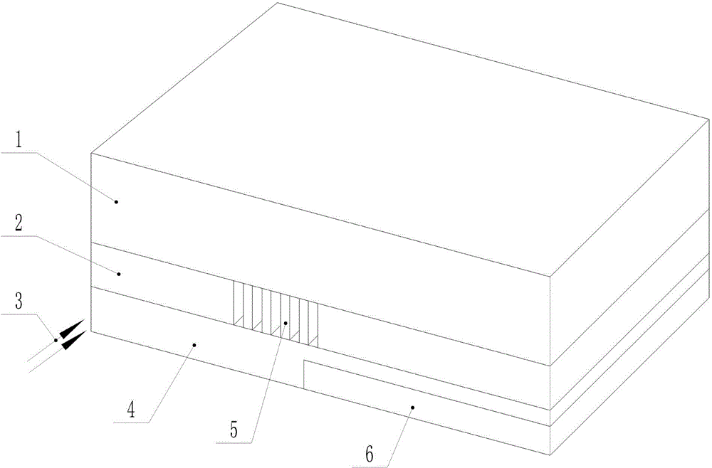
[0017] refer to figure 1 , a glass-loaded asymmetric SiO 2 -Gold film-SiO 2 Surface plasmon propagation device with waveguide structure including sequentially stacked top layers of SiO 2 Layer 1, gold film layer 2, L-shaped glass layer 4, bottom SiO 2 Layer 6, wherein the outer end surface of the L-shaped long side of the glass layer 4 is overlapped with the gold film layer 2, and the inner end surface of the L-shaped long side is connected to the bottom SiO 2 Layer 6 is spliced.

[0018] The outer end surface of the L-shaped long side of the glass layer 4 is to diffract the incident light into the gold film to excite the top layer of SiO 2 The surface plasmon resonance phenomenon between layer 1 and gold film layer 2, and the inner end surface of the L-shaped long side of glass layer 4 realizes the glass layer prism and the underlying SiO 2 Layer 6 undergoes total reflection to compensate for the effects of SPPs propagation loss.

[0019] The angle of incidence is great...


PUM

PropertyMeasurementUnit
Thicknessaaaaaaaaaa

Abstract

The invention discloses a glass-loaded asymmetric surface plasmon polariton spread device of a SiO2-gold film-SiO2 waveguide structure. The device is characterized by comprising a top SiO2 layer, a gold film layer, an L-shaped glass layer and a bottom SiO2 layer which are sequentially laminated, wherein the outer end face of the L-shaped long edge of the glass layer is laminated with the gold film layer; the inner end face of the L-shaped long edge is laminated with the bottom SiO2 layer; a grating structure is etched on the gold film layer; spread conduction type SPPs produced on the interface of the top SiO2 layer-gold film layer through excitation is enhanced by the grating structure. According to the device, the SPPs is excited by using the similar Kretschmann structure; the SPPs excitation is enhanced by using the grating structure; localization in the SPPs spread process is enhanced between glass and the SiO2 layer by total reflection by using reflected light of the gold film; the SPPs spread distance is meanwhile improved without sacrificing the sub-wavelength confinement of the waveguide. Key devices can be provided for application of the SPPs in the aspects such as novel photonic devices, wideband communication systems, tiny photonic circuits and optoelectronic integration; the device is low in cost and easy to implement.

Description

technical field [0001] The invention relates to optical communication technology, in particular to a glass-loaded asymmetric SiO 2 -Gold film-SiO 2 Surface plasmon propagation device with waveguide structure. Background technique [0002] Surface plasmon polaritons (SPPs for short) is an electromagnetic mode between a light wave and a migratable surface charge realized by changing the subwavelength structure of the metal surface, which can support the surface plasmon wave transmitted at the interface between the metal and the medium. Light energy is thus transmitted without being limited by the diffraction limit. Because of the unique properties of SPPs, it plays an important role in manipulating light energy at the nanoscale. Especially in the low temperature environment designed by Professor Oulton of Imperial College London, the covering thin MgF 2 The CdS nanowire structure is added to the silver film, and the experimental device is made of 15nm SiO 2 The ball is wr...

Claims


Application Information

Patent Timeline
IPC IPC(8): G02B6/122
CPCG02B6/122
Inventor 朱君秦柳丽宋树祥罗晓曙
Owner GUANGXI NORMAL UNIV
Learn More