A kind of LED structure and manufacturing method thereof
A technology of LED structure and manufacturing method, applied in electrical components, circuits, semiconductor devices, etc., can solve the problems of high LED chip voltage, poor reliability, separation of P pads and extended electrode LED die, etc., to improve the expansion effect, The effect of improving luminous uniformity
- Summary
- Abstract
- Description
- Claims
- Application Information
AI Technical Summary
Problems solved by technology
Method used
Image
Examples
Embodiment 1
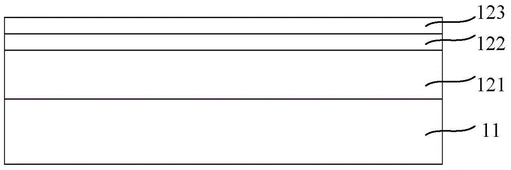
[0057] Such as Figure 1A As shown, an epitaxial wafer is provided. The epitaxial wafer includes a substrate 11 and a stacked epitaxial structure formed on the substrate 11. The stacked epitaxial structure includes an N-type epitaxial layer 121 and an active layer 122 from bottom to top. and a P-type epitaxial layer 123, the substrate 11 is, for example, a sapphire substrate.
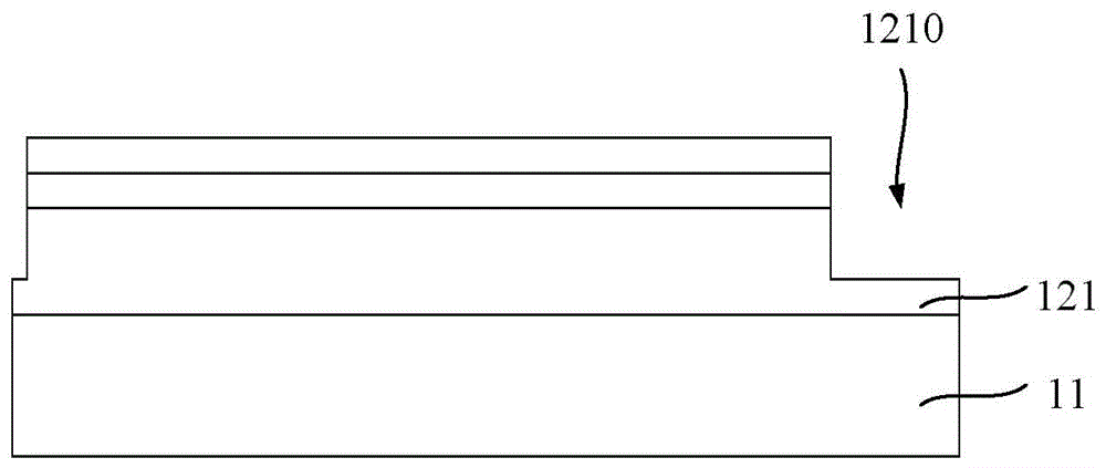
[0058] Such as Figure 1B As shown, an N-region mesa 1210 is fabricated on the stacked epitaxial structure through a conventional photolithography process, and the N-region mesa 1210 exposes the N-type epitaxial layer 121 . In this embodiment, the depth of the N-region mesa 1210 is greater than the sum of the thicknesses of the active layer 122 and the P-type epitaxial layer 123 but less than the sum of the thicknesses of the stacked epitaxial structure, that is, the thickness of the N-type epitaxial layer 121 The thickness of the N-type epitaxial layer 121 is smaller than that of other regions.
[0...
Embodiment 2
[0075] The difference between this embodiment and the first embodiment is that a high-resistance ITO thin film is formed on the P-type epitaxial layer by evaporation, and then an ITO barrier layer is formed by photolithography. In this embodiment, the high-temperature annealing process can be omitted, and a high-resistance ITO thin film is directly formed on the P-type epitaxial layer by controlling the evaporation power, evaporation temperature, and one or more methods in the oxygen atmosphere of the evaporation chamber during the evaporation process. , and then etch to form an ITO pattern to form a high-resistance ITO barrier layer.
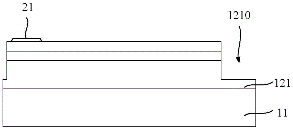
[0076] Specifically, in this embodiment, combined with Figure 1A-1F Firstly, a high-resistance ITO film is formed on the P-type epitaxial layer 123 by evaporation, and a high-resistance ITO film can be formed by increasing the evaporation power, reducing the evaporation temperature, and increasing the oxygen atmosphere in the evaporation chambe...
Embodiment 3
[0080]The difference between this embodiment and Embodiment 1 is that while the ITO barrier layer 21 is formed on the P-type epitaxial layer 123 at the position corresponding to the P pad, an array of ITO barriers is also formed on the P-type epitaxial layer 123. The auxiliary layer 22 is extended. combine Figure 2A-2F As shown, in this embodiment, an ITO thin film is formed on the P-type epitaxial layer 123 by evaporation, and an ITO barrier layer pattern and an extended auxiliary layer pattern are simultaneously formed by photolithography and etching processes, and then a fluorine-containing solution is used Process the ITO barrier layer pattern and the extended auxiliary layer pattern, and carry out high-temperature annealing treatment to the ITO barrier layer pattern and the extended auxiliary layer pattern, so that the resistance of the ITO barrier layer pattern and the extended auxiliary layer pattern becomes large (conductivity variation) to simultaneously form the IT...
PUM
 Abstract
Description
Claims
Application Information
 - R&D
- Intellectual Property
- Life Sciences
- Materials
- Tech Scout
- Unparalleled Data Quality
- Higher Quality Content
- 60% Fewer Hallucinations
Browse by: Latest US Patents, China's latest patents, Technical Efficacy Thesaurus, Application Domain, Technology Topic, Popular Technical Reports.
© 2025 PatSnap. All rights reserved.Legal|Privacy policy|Modern Slavery Act Transparency Statement|Sitemap|About US| Contact US: help@patsnap.com


