Multibus bus-to-ISA bus read-write operation switching circuit
A technology for reading and writing operations and converting circuits, which is applied in the field of reinforced computer design, can solve the problems of inability to achieve mixed insertion and compatibility, and achieve the effects of improving system testing capabilities, occupying less resources, and simple circuit structure
- Summary
- Abstract
- Description
- Claims
- Application Information
AI Technical Summary
Problems solved by technology
Method used
Image
Examples
Embodiment Construction
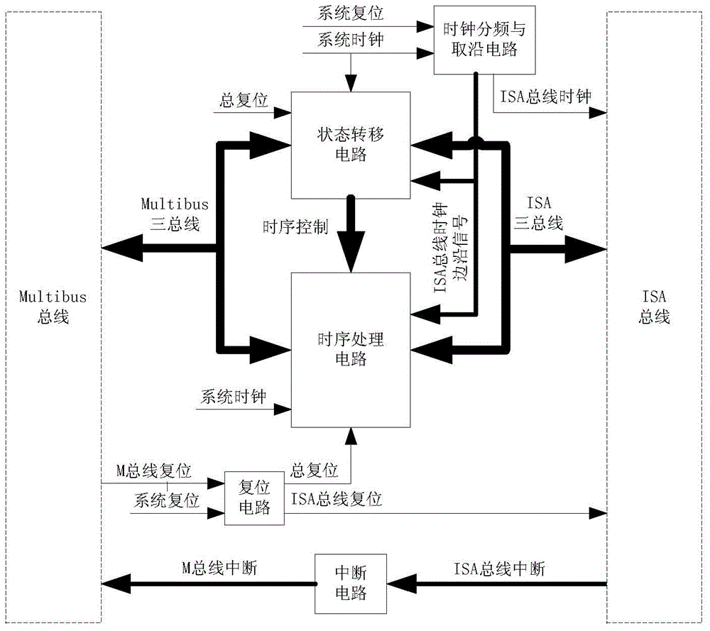
[0025] combined with figure 1 , illustrate the composition of the multibus bus of the present invention to the composition of the read and write operation conversion circuit of ISA bus.
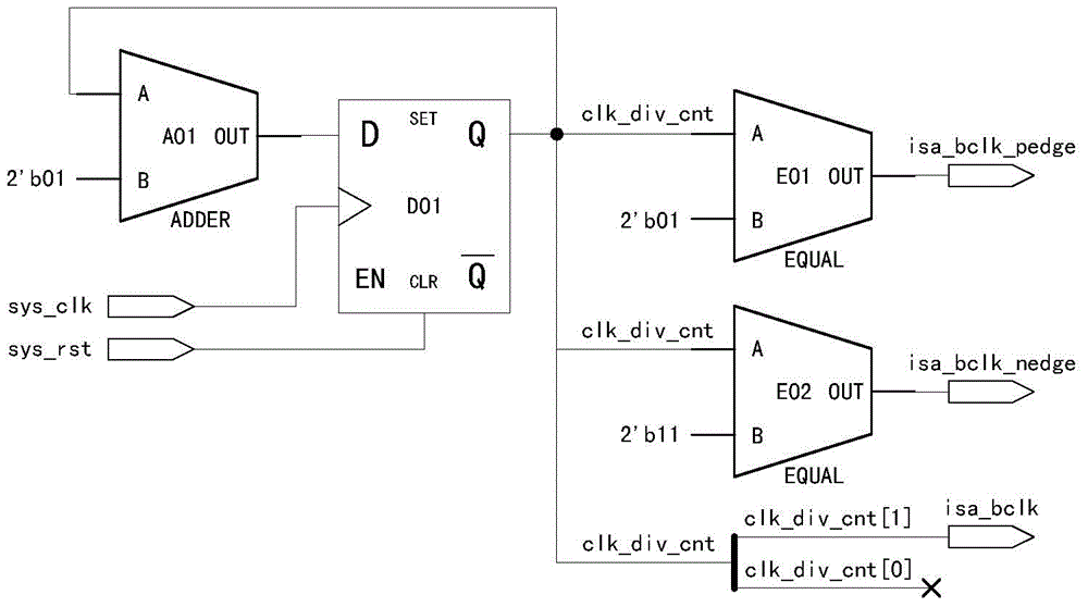
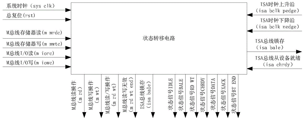
[0026] A read and write operation conversion circuit from a Multibus bus to an ISA bus of the present invention includes a clock frequency division and edge fetching circuit, a state transfer circuit, a sequence processing circuit, a reset circuit, and an interruption circuit; the clock frequency division and edge fetching circuit receives a system clock With the system reset signal, output the ISA bus clock edge signal to the state transfer circuit and timing processing circuit, and output the ISA bus clock to the ISA bus, the core part of the Multibus bus. Multibus three buses (control bus, address bus, data bus) and state transfer The circuit is connected to the timing processing circuit, the Multibus bus interrupt signal is connected to the interrupt circuit, the state transfer circuit ou...
PUM
 Abstract
Description
Claims
Application Information
 - R&D
- Intellectual Property
- Life Sciences
- Materials
- Tech Scout
- Unparalleled Data Quality
- Higher Quality Content
- 60% Fewer Hallucinations
Browse by: Latest US Patents, China's latest patents, Technical Efficacy Thesaurus, Application Domain, Technology Topic, Popular Technical Reports.
© 2025 PatSnap. All rights reserved.Legal|Privacy policy|Modern Slavery Act Transparency Statement|Sitemap|About US| Contact US: help@patsnap.com


