Method for reducing diameter of self-crimping micron tube by virtue of metal nanoparticles
A metal nanoparticle, self-curling technology, applied in metal material coating technology, microstructure technology, microstructure device and other directions, can solve problems such as unsatisfactory effects, achieve excellent mechanical properties and structural properties, and improve SERS) strength , the effect of reducing the diameter
- Summary
- Abstract
- Description
- Claims
- Application Information
AI Technical Summary
Problems solved by technology
Method used
Image
Examples
Embodiment 1
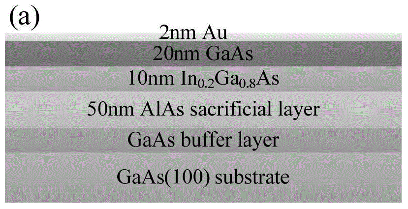
[0050]Embodiment 1 of the present invention provides a method for reducing the diameter of self-curling microtubes by means of metal nanoparticles. The process flow is shown in Figure 1, which specifically includes the following steps:
[0051] S1: Deposit a GaAs buffer layer on a GaAs(100) single crystal substrate:
[0052] In arsine (AsH 3 ) to 720°C under protection, using the MOCVD method, using trimethylgallium (TMGa) and AsH 3 GaAs buffer layer is grown. The thickness of the GaAs buffer layer is 400nm, and the V / III ratio is controlled at 60.
[0053] S2: Growing a sacrificial layer on the GaAs buffer layer:
[0054] At 720°C, with trimethylaluminum (TMAl) and AsH 3 An AlAs sacrificial layer is grown. The thickness of the AlAs sacrificial layer is 50nm, and the V / III ratio is controlled at 40.
[0055] S3: Growth of the strained film on the sacrificial layer:
[0056] At 720°C, using trimethylindium (TMIn), TMGa and AsH 3 GrowthIn x Ga 1-x As / GaAs strained bila...
Embodiment 2
[0081] The preparation method is the same as in Example 1, and the difference is HF in the S8 step: H 2 The etching time of O=1:40 (volume ratio) solution to laterally etch the AlAs sacrificial layer (without stirring at room temperature) was increased to 120s.
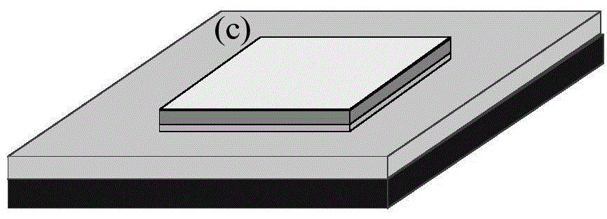
[0082] When rolled into a multi-coil tube, nano-gold particles are embedded in the tube wall, forming a semiconductor / metal nanoparticle heterostructure (such as image 3 (c) as shown in the SEM image).
Embodiment 3
[0084] S3: Growth of the strained film on the sacrificial layer:
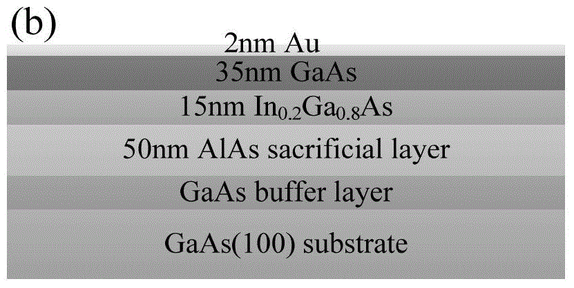
[0085] The composition x of In is controlled at 0.2, the thickness of InGaAs / GaAs is 15nm / 35nm respectively, and the ratio of V / III is controlled at 60. Figure 1(b) The epitaxial wafer structure used to prepare self-curling microtubes on a GaAs(100) substrate, on which a 2nm thick Au film is deposited on the surface, and the bottom layer is a GaAs(100) substrate.
[0086] S7: using rapid thermal annealing (RTA) to make the metal film form metal nanoparticles;
[0087] In nitrogen (N 2 ) atmosphere for In with a thickness of 15nm / 35nm 0.2 Ga 0.8 The As / GaAs strained film was subjected to RTA, and the annealing temperature was maintained at 650°C for 300s; Figure 4(a) and Figure 4(b): The 2nm thick gold film on the surface of the InGaAs / GaAs strained film was subjected to rapid thermal annealing to form gold nanoparticles.
[0088] 15nm / 35nm In 0.2 Ga 0.8 The SEM of the As / GaAs strained bilayer film after s...
PUM
| Property | Measurement | Unit |
|---|---|---|
| thickness | aaaaa | aaaaa |
| diameter | aaaaa | aaaaa |
| length | aaaaa | aaaaa |
Abstract
Description
Claims
Application Information
 - R&D
- Intellectual Property
- Life Sciences
- Materials
- Tech Scout
- Unparalleled Data Quality
- Higher Quality Content
- 60% Fewer Hallucinations
Browse by: Latest US Patents, China's latest patents, Technical Efficacy Thesaurus, Application Domain, Technology Topic, Popular Technical Reports.
© 2025 PatSnap. All rights reserved.Legal|Privacy policy|Modern Slavery Act Transparency Statement|Sitemap|About US| Contact US: help@patsnap.com


