
LCD panel

A display panel and display area technology, applied in nonlinear optics, instruments, optics, etc., can solve the problems of positional accuracy variation, difficult control of cutting accuracy, uneven section of liquid crystal display panel, etc., to meet the needs of easy design and improve product quality rate effect

Active Publication Date: 2018-01-23
AU OPTRONICS CORP
View PDF6 Cites 0 Cited by
  • Summary
  • Abstract
  • Description
  • Claims
  • Application Information

AI Technical Summary

Problems solved by technology

Because the glue width and position accuracy often change when the frame glue is applied, the design of the ultra-thin frame will cause the frame glue to easily shift to the cutting line or be pressed against the two corresponding substrates of the LCD panel. After closing, the frame glue overflows to the cutting line
In the process of cutting and slicing after curing the frame glue, the cutting precision is difficult to control due to the formation of cured frame glue on the cutting line, and it is easy to cause the liquid crystal display panel to fail to be broken smoothly or the junction of the sections to form concave and convex angles during cutting. Bad problems arise
Therefore, the edge of the obtained liquid crystal display panel is prone to uneven sections, which in turn affects the processing accuracy and the yield rate of the subsequent manufacturing process.

Method used


Image

  • LCD panel
  • LCD panel
  • LCD panel

Examples


Embodiment Construction

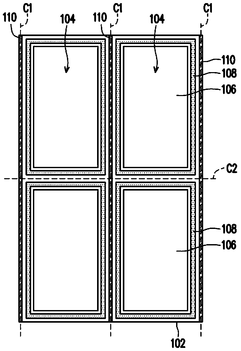
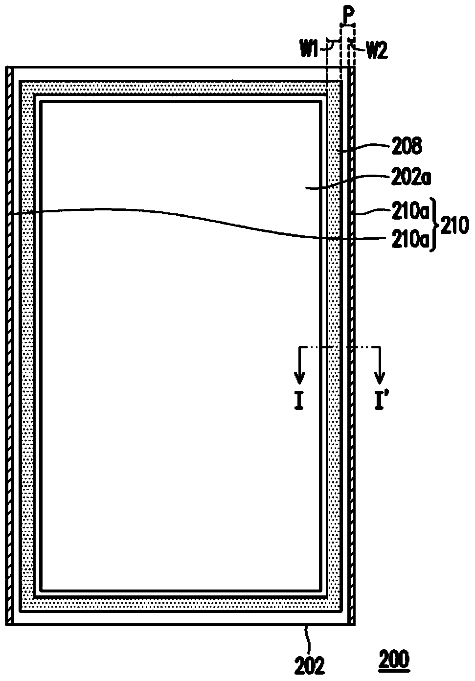
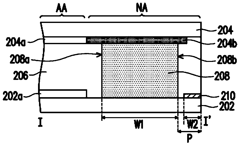
[0060] Generally speaking, a liquid crystal display panel is mainly composed of two substrates and a liquid crystal layer sandwiched between the two substrates. Based on the consideration of mass production efficiency, multiple liquid crystal display panels are efficiently produced. In the production process, multiple liquid crystal display panels are usually formed on two large mother substrates. Each liquid crystal display panel includes active components, for example. array, color filter pattern, black matrix and other required component structures, two mother substrates are bonded together and injected into the liquid crystal layer to complete the production of multiple liquid crystal display panels at the same time. Afterwards, the laminated mother substrate is cut into a plurality of independent liquid crystal display panels (or called liquid crystal display units) through cutting and slitting processes.

[0061] figure 1 is a schematic top view of a motherboard accordi...


PUM


Abstract

The invention discloses a liquid crystal display panel, which includes a first substrate, a second substrate, a liquid crystal layer, a light-curing sealant and a first light-shielding pattern. The liquid crystal layer is arranged between the first substrate and the second substrate. The light-curing sealant is disposed between the first substrate and the second substrate, wherein the light-curing sealant surrounds and contacts the liquid crystal layer. The first light-shielding pattern is arranged on the first substrate, wherein part of the sidewalls of the first light-shielding pattern is substantially flush with part of the sidewalls of the first substrate, and the first light-shielding pattern only overlaps with an outer edge of the light-curing frame glue or the first light-shielding pattern. A light-shielding pattern does not overlap with the light-curing frame glue.

Description

[0001] This application is a divisional application of the patent application for invention filed on August 16, 2010, with the name "Liquid Crystal Display Panel" and application number 201010256077.7. technical field [0002] The present invention relates to a display panel, and in particular to a liquid crystal display panel. Background technique [0003] With the advancement of display technology, people can make their lives more convenient with the assistance of displays. In order to achieve the characteristics of lightness and thinness of displays, flat panel displays (FPDs) have become the current mainstream. Among many flat panel displays, a liquid crystal display (LCD) has superior characteristics such as high space utilization efficiency, low power consumption, no radiation, and low electromagnetic interference, so the liquid crystal display is very popular among consumers. [0004] In order to mass-produce liquid crystal displays, the size of the glass substrate us...

Claims


Application Information

Patent Timeline
Patent Type & Authority Patents(China)
IPC IPC(8): G02F1/1335G02F1/1339
CPCG02F1/133512G02F1/1339
Inventor 杨伟杰徐文义简维谊黄美莲蔡蔚珍刘昱辰曾至孝
Owner AU OPTRONICS CORP
Learn More