
Flip chip led chip

A LED chip, flip-chip technology, applied in the direction of semiconductor devices, electrical components, circuits, etc., can solve problems such as short circuit, electrical metal overflowing the electrode surface, on the same electrode, or on two electrodes at the same time, etc. Achieve the effect of improving packaging yield, avoiding mutual conduction, and better soldering effect

Active Publication Date: 2019-08-13
刘艳
View PDF5 Cites 0 Cited by
  • Summary
  • Abstract
  • Description
  • Claims
  • Application Information

AI Technical Summary

Problems solved by technology

Flip-chip LED chips with the existing structure cannot be produced by traditional LED automatic die-bonding machines, or conductive metal appears on the same electrode or on two electrodes at the same time when using traditional LED automatic die-bonding machines to produce The phenomenon, or the phenomenon of short circuit due to the overflow of conductive metal from the surface of the electrode due to the small size of one electrode
These all affect the packaging yield of LED

Method used


Image

  • Flip chip led chip
  • Flip chip led chip
  • Flip chip led chip

Examples


Embodiment Construction

[0034] Various exemplary embodiments, features, and aspects of the invention will be described in detail below with reference to the accompanying drawings. The same reference numbers in the figures indicate functionally identical or similar elements. While various aspects of the embodiments are shown in drawings, the drawings are not necessarily drawn to scale unless specifically indicated.

[0035] The word "exemplary" is used exclusively herein to mean "serving as an example, embodiment, or illustration." Any embodiment described herein as "exemplary" is not necessarily to be construed as superior or better than other embodiments.

[0036] In addition, in order to better illustrate the present invention, numerous specific details are given in the specific embodiments below. It will be understood by those skilled in the art that the present invention may be practiced without certain of the specific details. In other instances, methods, means, components and circuits well k...


PUM


Abstract

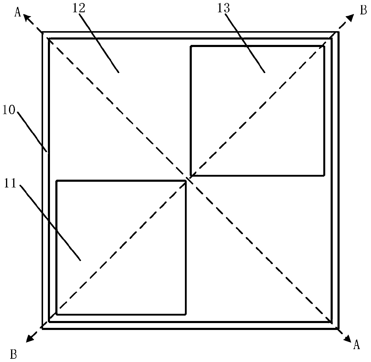
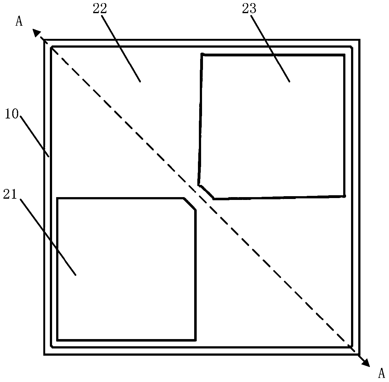
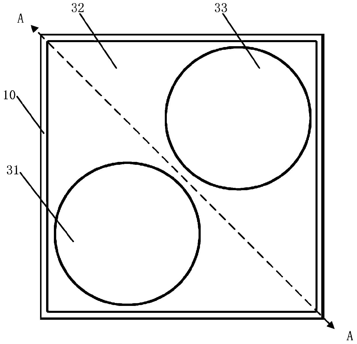
The invention discloses a flip chip type LED chip. The flip chip type LED chip comprises a substrate, and an anode, an isolation region and a cathode which are sequentially arranged at a front face of the substrate along the horizontal direction, wherein the horizontal direction is parallel with the front face of the substrate, the vertical projection of the isolation region on the front face of the substrate is between vertical projections of the anode and the cathode on the front face of the substrate, and the center line of the isolation region on the horizontal direction and the vertical projection of a diagonal line of the flip chip type LED chip on the front face of the substrate are mutually overlapped. According to the flip chip type LED chip, the distance from the anode to the cathode can be made to be longest, the optimum welding effect can be realized when a traditional LED automatic chip die bonder is utilized for production, and thereby mutual conduction of the anode and the cathode can be avoided during packaging of flip chip LEDs, and the packaging yield rate of the flip chip LEDs is improved.

Description

technical field [0001] The invention relates to the technical field of light-emitting elements, in particular to a flip-chip LED chip. Background technique [0002] With the increasing development of LED (Light Emitting Diode, light emitting diode) lighting technology, the application of LED in people's daily life is also becoming more and more extensive. [0003] Flip Chip (Flip Chip) packaged LEDs (hereinafter referred to as flip-chip LEDs) have a simple die-bonding method and higher reliability, which greatly improves the feasibility of mass production and shortens the high-temperature baking process. The advantages of time, high yield, good thermal conductivity, and high light output have become the technologies that the industry is striving to develop. [0004] Flip-chip LED chips are soldered by soldering gold balls, tin balls, or eutectic soldering on the structure of the substrate to which the positive electrodes and negative electrodes of the flip-chip LED chips ar...

Claims


Application Information

Patent Timeline
Patent Type & Authority Patents(China)
IPC IPC(8): H01L33/38H01L33/46H01L33/62
CPCH01L33/38H01L33/44H01L33/46H01L33/62
Inventor 吴裕朝刘艳
Owner 刘艳
Learn More