a semiconductor device

A semiconductor and device technology, which is applied in the field of semiconductor preparation, can solve the problems that electric fuses are difficult to completely blown, electric fuse conductive plugs are prone to damage, and electric fuse fuses have low yields.

Active Publication Date: 2017-05-17
SEMICON MFG INT (SHANGHAI) CORP
View PDF6 Cites 0 Cited by
  • Summary
  • Abstract
  • Description
  • Claims
  • Application Information

AI Technical Summary

Problems solved by technology

[0009] The problem solved by the present invention is to provide a semiconductor device to overcome the problems that the existing electric fuse is difficult to completely blown, the yield rate of the electric fuse is low, and the conductive plug on the electric fuse is easily damaged.

Method used


Image

  • a semiconductor device
  • a semiconductor device
  • a semiconductor device

Examples


preparation example Construction

[0072] The preparation process of the above-mentioned conductive plug may include:

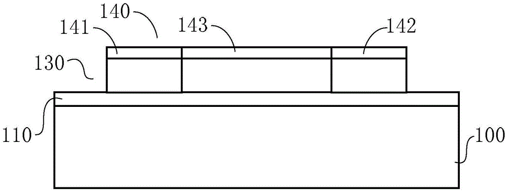
[0073] refer to Figure 10 As shown, after the conductive layer 140 is formed, a dielectric layer 160 is formed above the insulating layer 110 and the conductive layer 140, and the dielectric layer 160 can be selected from dielectric materials such as silicon oxide, silicon nitride, and silicon oxynitride. .

[0074] In this embodiment, the material of the dielectric layer 160 is silicon oxide, and its formation process is CVD (Chemical Vapor Deposition).

[0075] refer to Figure 11 As shown, in the dielectric layer 160, a first through hole 161 and a second through hole 162 are opened above the cathode 141 and the anode 142 of the conductive layer 140 until the cathode 141 and the anode 142 are exposed.

[0076] The specific process of opening the first through hole 161 and the second through hole 162 includes covering a hard mask layer (not shown in the figure) and a photoresist layer (n...

Embodiment

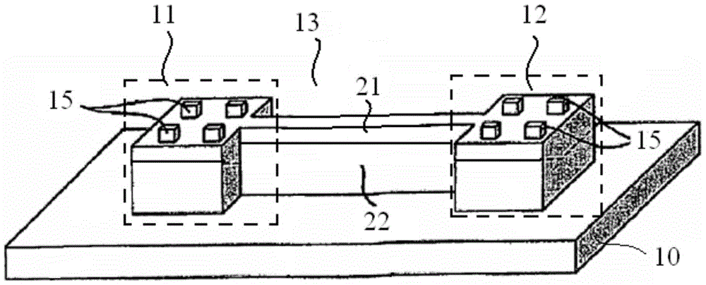
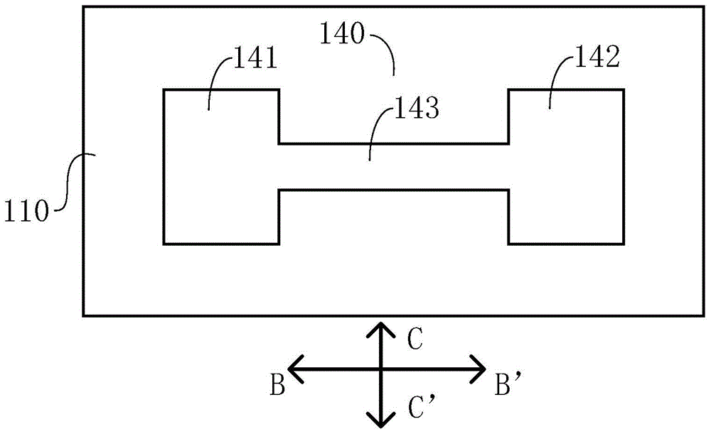
[0083] Embodiment: One above-mentioned conductive plug with a "T" structure is arranged on each of the anode and the cathode, wherein the width of the end is 160 nm, and the length is 80 nm; the width of the neck is 30 nm, and the length is 80 nm.


PUM


Abstract

The invention provides a semiconductor device which comprises an electric fuse positioned on the surface of a semiconductor substrate, and a first conductive plug and a second conductive plug which are respectively positioned on a positive electrode and a negative electrode of the electric fuse, wherein each of the first conductive plug and the second conductive plug comprises an end part and a neck part; the end parts are arranged in a manner of being close to a middle section, and the neck parts are arranged in a manner of being far away from the middle section; the widths of the first conductive plug and the second conductive plug in the direction perpendicular to the middle section of the electric fuse are greater than the widths of the neck parts. After voltage is applied to the first conductive plug and the second conductive plug, current is concentrated to the end parts, and heat generated on the first conductive plug and the second conductive plug is concentrated to the end parts, so that the fusing rate of the middle section of the electric fuse is increased.

Description

technical field [0001] The invention relates to the field of semiconductor preparation, in particular to a semiconductor device. Background technique [0002] In the field of integrated circuits, an electric fuse (Fuse) refers to a connection line that can change greatly in resistance (from a low-resistance state to a high-resistance state) or can be blown in an integrated circuit. [0003] The main uses of electric fuses include: (1) It is used to start redundant circuits to replace defective circuits on the same chip, thereby effectively improving the process yield. The redundant circuit in the integrated circuit is connected by electric fuse. Once the integrated circuit is found to be defective, the electric fuse can be used to repair or replace the defective circuit; (2) It is used for the programming function of the integrated circuit. The electric fuse is set on the programming circuit. During the programming process of the integrated circuit, the electric fuse is blo...

Claims


Application Information

Patent Timeline
Patent Type & Authority Patents(China)
IPC IPC(8): H01L23/525
Inventor 廖淼
Owner SEMICON MFG INT (SHANGHAI) CORP
Why Eureka
Try Eureka