An external cavity semiconductor laser optical path adjustment device and adjustment method

An optical path adjustment and semiconductor technology, which is applied in the field of external cavity semiconductor laser optical path adjustment devices, can solve the problems of difficulty in obtaining the optimal state of the external cavity optical path, and it is difficult to achieve the optimal coupling between the internal cavity and the external cavity, and achieves strong practical value, improves power, and improves The effect of adjusting the precision

Active Publication Date: 2018-04-27
XIAMEN UNIV
View PDF14 Cites 0 Cited by
  • Summary
  • Abstract
  • Description
  • Claims
  • Application Information

AI Technical Summary

Problems solved by technology

In the process of debugging the optical path of the external cavity with the traditional method, the size and specific position of the light spot on the cavity surface of the feedback semiconductor gain device cannot be judged. optimal coupling

Method used


Image

  • An external cavity semiconductor laser optical path adjustment device and adjustment method
  • An external cavity semiconductor laser optical path adjustment device and adjustment method

Examples


Embodiment 1

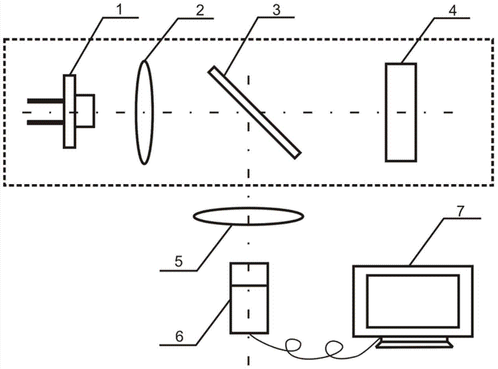
[0029] see figure 1 , The embodiment of the external cavity semiconductor laser optical path adjustment device is provided with a semiconductor gain device 1, a collimating lens 2, a beam splitter 3, a light splitting element 4, a focusing lens 5, a CCD camera 6 and a display screen 7.

[0030] The semiconductor gain device 1, collimating lens 2, beam splitter 3, and light splitting element 4 are arranged coaxially in sequence, the focusing lens 5 and the CCD camera 6 are arranged on the reflected light path of the beam splitter 3 in turn, and the output port of the CCD camera 6 Connect to the input terminal of display screen 7.

[0031] The semiconductor gain device 1 is a semiconductor light-emitting device with optical gain, including but not limited to edge-emitting semiconductor lasers, superluminescent light-emitting diodes, optical amplifiers, and the like.

[0032] The collimator lens 2 is an optical lens with optical collimation function, which can collimate the beam...

Embodiment 2

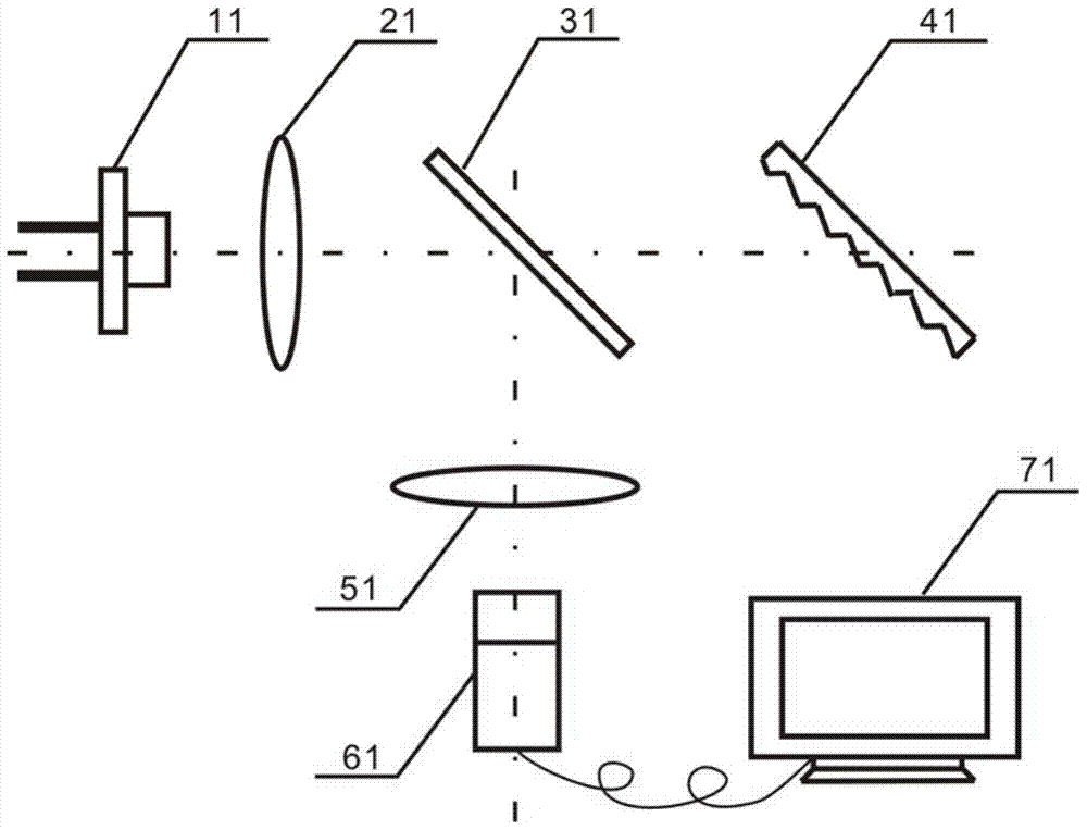
[0049] Such as figure 2 As shown, similar to Embodiment 1, the difference is that the light splitting element adopts a diffraction grating 41, and the present invention is applied to the optical path of a Littrow-type grating external cavity semiconductor laser, which mainly includes: a semiconductor gain device 11, a collimating lens 21, beam splitter 31 , diffraction grating 41 , focusing lens 51 , CCD camera 61 and display screen 71 .

[0050] The semiconductor gain device 11 is a semiconductor light emitting device with optical gain, and an edge-emitting semiconductor laser diode coated with an anti-reflection film on the surface of the optical cavity can be selected.

[0051] The collimator lens 21 is an optical lens with optical collimation function, which can collimate the beam emitted by the semiconductor gain device 11 into a parallel beam, and an aspheric lens with a numerical aperture of 0.5 can be selected.

[0052] The beam splitter 31 is an optical element with...


PUM


Abstract

The invention provides an adjustment device and method for an optical path of an external cavity semiconductor laser, and relates to an external cavity semiconductor laser. The adjustment device comprises a semiconductor gain device, a collimating lens, a beam splitter, a light splitting element, a focusing lens, a CCD camera and a display screen. The adjustment method comprises the following steps: firstly, moving the beam splitter into the optical path; emitting laser light after lasing by the semiconductor gain device to the beam splitter after alignment; with the multistage diffraction of transmitted light on the light splitting element, feeding back primary diffracted light to a position near to a cavity surface of an internal cavity of the semiconductor gain device by regulating the angle of the light splitting element; focusing the reflected light passing through the beam splitter in the CCD camera by regulating the focusing lens, and regulating the size and the location of a feedback light spot by performing multidimensional state micro-adjustment on the collimating lens and the light splitting element; finally, enabling the feedback light spot to be completely overlapped with the cavity surface of the internal cavity, and then obtaining an optimum state of the optical path of the external cavity laser; and after the completion of optical path adjustment, removing the beam splitter from the optical path to avoid the output light loss of the external cavity laser.

Description

technical field [0001] The invention relates to an external cavity semiconductor laser, in particular to an external cavity semiconductor laser for observing and analyzing the external cavity feedback light spot and the internal cavity surface of a semiconductor gain device by adding a micro-region image analysis optical path to the optical path of the external cavity semiconductor laser Optical path adjustment device and adjustment method. Background technique [0002] External cavity semiconductor lasers are a type of laser light source made with external optical components as optical feedback and mode selection components. This type of laser light source has the advantages of high spectral purity, tunable lasing wavelength, high efficiency, and good reliability. Communication, optical measurement, optical storage and other fields have broad application prospects. Among them, accurately feeding the external feedback light back to the active region of the semiconductor gai...

Claims


Application Information

Patent Timeline
Patent Type & Authority Patents(China)
IPC IPC(8): H01S5/14H01S5/06
Inventor 吕雪芹王霏
Owner XIAMEN UNIV
Why Eureka
Try Eureka