Photoresist edge cleaning device and method

A cleaning device and photoresist technology, applied in the processing of photosensitive materials, etc., can solve the problems of high solvent material consumption, high photoresist, and productivity impact, etc., and achieve the effect of improving removal time, improving efficiency, and reducing the amount of consumption.

Active Publication Date: 2015-03-04
NANTONG FUJITSU MICROELECTRONICS
View PDF7 Cites 12 Cited by
  • Summary
  • Abstract
  • Description
  • Claims
  • Application Information

AI Technical Summary

Problems solved by technology

Therefore, a lot of photoresist needs to be removed, and it takes about 3 to 5 minutes to remove the edge of a wafer, which affects the production capacity and consumes a lot of solvent materials.

Method used


Image

  • Photoresist edge cleaning device and method
  • Photoresist edge cleaning device and method
  • Photoresist edge cleaning device and method

Examples


Embodiment Construction

[0027] The present invention will be described in further detail below in conjunction with the accompanying drawings and embodiments. It should be understood that the specific embodiments described here are only used to explain the present invention, not to limit the present invention.

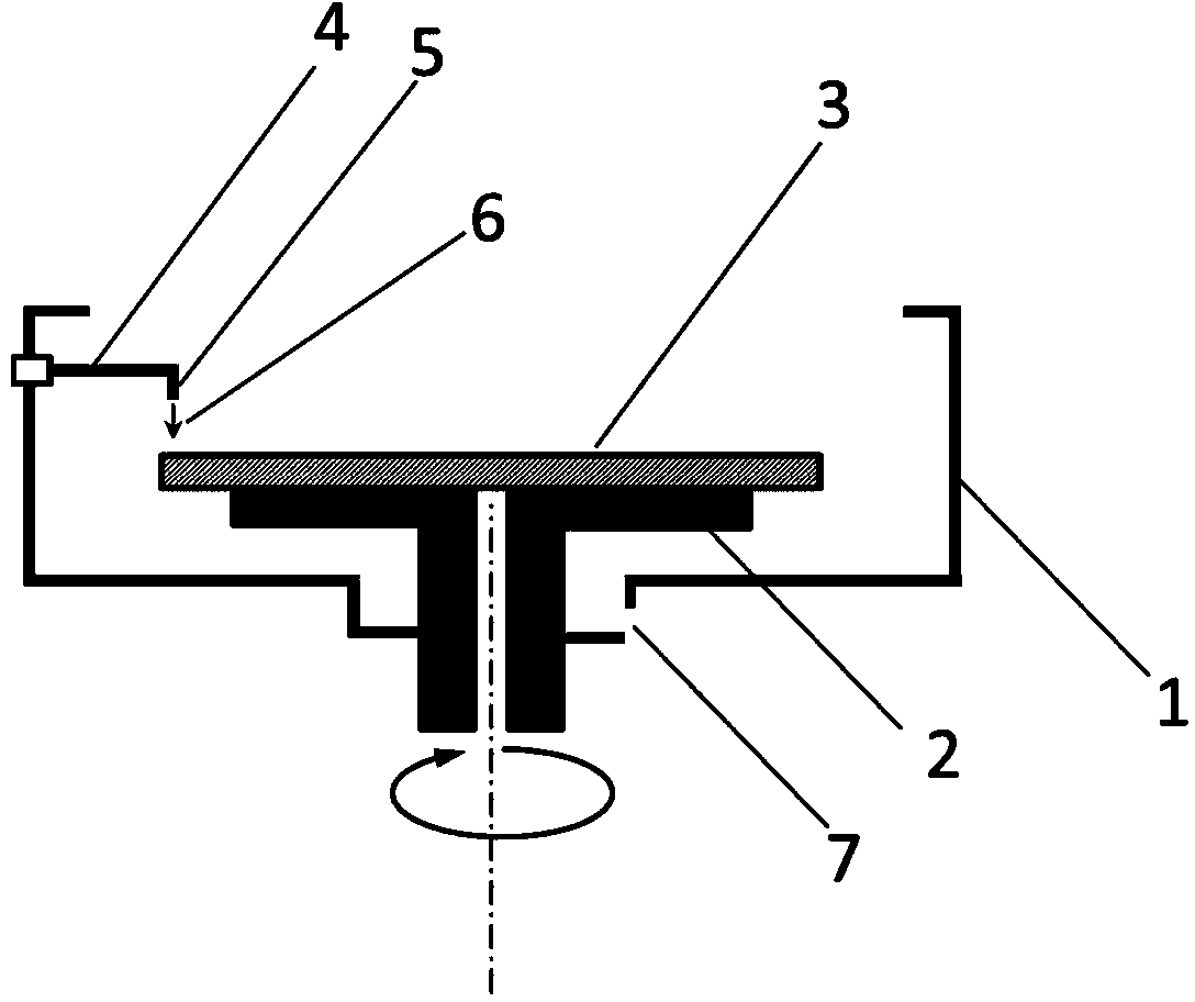
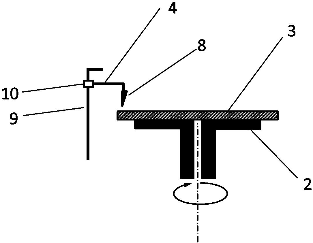
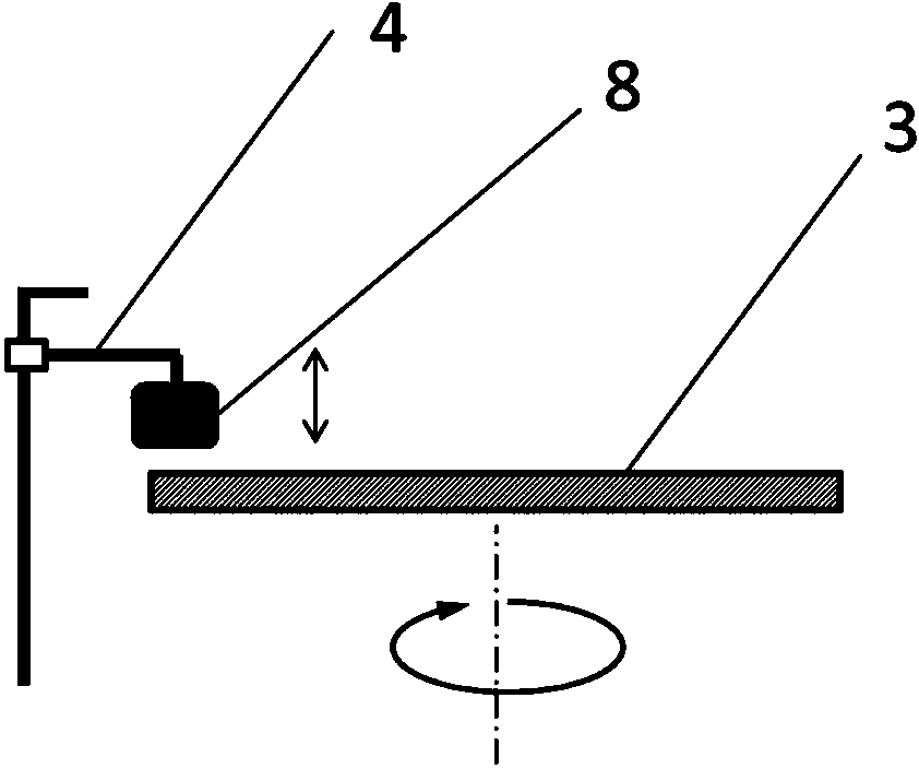
[0028] In the first embodiment of the present invention, a photoresist edge cleaning device is provided, which includes: a rotary table 2, which can be a vacuum chuck. When working, the rotary table 2 rotates around the central axis to generate centrifugal force so that the photolithography The glue or photoresist glue is evenly distributed on the wafer 3 step by step. The rotary table 2 is driven by a multistage motor (not shown in the figure). A solvent pipe 4 is used to transport solvent. The solvent pipe is a hollow tubular structure. The solvent pipe 4 is connected with a scraper 8. The solvent pipe is connected with the EBR moving arm 9, and the EBR moving arm is in the servo mechanism ...


PUM


Abstract

The invention provides a photoresist edge cleaning device and method. The photoresist edge cleaning device comprises a solvent pipe 4 used for conveying a solvent, and is characterized in that the solvent pipe 4 is connected with a scraper 8. The photoresist edge cleaning method comprises the following steps: photoresist on a wafer is removed physically; and the photoresist on the wafer is removed chemically. After the scraper 8 moves downward to scrap off the photoresist on the wafer 3, a pinhead located on or in the scraper 8 sprays the solvent, and residual photoresist on the bottom layer of the wafer 3 reacts with the solvent agent. Compared with the prior art, the edge photoresist removal time can be shortened remarkably, the use amount of the chemical solvent is reduced while the efficiency is increased, and the cost decreasing and benefit increasing function is realized.

Description

technical field [0001] The invention relates to the technical field of semiconductor photolithography, in particular to a photoresist edge cleaning device and method. Background technique [0002] Photolithography is a technology of image duplication and a key process technology in the integrated circuit manufacturing process. To put it simply, photolithography is to use photocopying method to accurately copy the pattern on the mask plate to the photoresist (hereinafter collectively referred to as photoresist) coated on the surface of the silicon wafer, and then print it on the surface of the photoresist. Perform ion implantation, etching (dry, wet), metal evaporation, etc. on silicon wafers under protection. During the manufacturing process of the wafer, various physical components of transistors, diodes, capacitors, resistors and metal layers are formed on the surface or in the surface layer of the wafer. These components are formed on one mask layer at a time, and combi...

Claims


Application Information

Patent Timeline
Patent Type & Authority Applications(China)
IPC IPC(8): G03F7/42
Inventor 丁万春
Owner NANTONG FUJITSU MICROELECTRONICS
Why Eureka
Try Eureka