Spin injector device comprising a protection layer at the centre thereof

A technology of spin injection and protective layer, applied in the field of electronics and spin electronics

Active Publication Date: 2015-02-25
CENT NAT DE LA RECH SCI (C N R S) +1
View PDF4 Cites 2 Cited by
  • Summary
  • Abstract
  • Description
  • Claims
  • Application Information

AI Technical Summary

Problems solved by technology

For this reason, current generation techniques are limited only to certain components

Method used


Image

  • Spin injector device comprising a protection layer at the centre thereof
  • Spin injector device comprising a protection layer at the centre thereof
  • Spin injector device comprising a protection layer at the centre thereof

Examples


Embodiment Construction

[0061] One of the objectives of the present application is to make a device for injecting materials that deflect spins when connected to a current source easy to manufacture. Devices of this type are also known as spin injection devices.

[0062] It is convenient when a manufacturing method is adapted to industrial requirements that it is easy and / or fast and / or can be realized economically while being reproducible on a large scale.

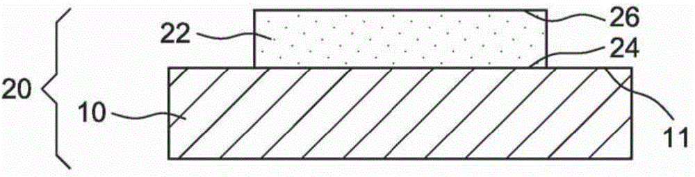
[0063] The spin injection device 30 includes a first material, referred to as the substrate 10 , which is electrically conductive and has magnetic properties. The first side 11 of the substrate 10 is in contact with the external environment and has magnetic properties of the ferromagnetic and / or ferrimagnetic and / or antiferromagnetic type ( figure 1 ).

[0064] The first side 11 of the substrate can, for example, comprise or be based on oxides and / or nitrides and / or carbides, or on cobalt and / or iron, and / or nickel. The term "based on" defines...


PUM


Abstract

The invention relates to a method for producing a spin injector device (30), comprising the following steps: a) formation of a metal protection layer (22) on a surface (11) of a substrate (10) such as to limit or prevent the oxidation and / or contamination of the surface by its environment, said surface being magnetic and electroconductive, the protection layer being naturally diamagnetic or paramagnetic; and b) formation of an upper layer (32) on the protection layer, which can stimulate a spin polarization, at close to the Fermi level, of the electronic states of the interface between the protection layer and the upper layer using an amplitude and a spin referential defined by the magnetism of the substrate and / or of the surface of the substrate, the upper layer being an organic layer and at least one of the molecular sites of said organic layer having a paramagnetic moment upon contact with the protection layer.

Description

technical field [0001] The present invention relates to the field of electronic technology, more precisely to the field of spintronic technology. In particular, the present invention relates to a method for manufacturing a spin injection device capable of filtering electrons flowing through the spin injection device according to the different spin orientations of the electrons. Background technique [0002] Technological advancements in the semiconductor industry have allowed for significant reductions in the size, and therefore increase in power and complexity, of electronic devices. Fabricating these devices at the atomic scale today presents new problems to overcome, especially with regard to the physical phenomena that occur at this scale. In order to further improve the performance of semiconductors, it is necessary to develop devices on the basis of new concepts. [0003] One of these concepts is to exploit the quantum properties of electron spin to store information...

Claims


Application Information

Patent Timeline
Patent Type & Authority Applications(China)
IPC IPC(8): H01F10/00H01F10/32H01F41/32
CPCH01L43/12H01L43/10H01F10/3254H01F41/32H01F10/005H10N50/85H10N50/01
Inventor 马丁·鲍恩米拜尔克·阿罗瓦尼萨米·布加里埃里克·博勒佩尔沃尔夫冈·韦伯法布里斯·朔伊雷尔罗伊克·兆丽
Owner CENT NAT DE LA RECH SCI (C N R S)
Why Eureka
Try Eureka