Semiconductor wafer cooling apparatus
A cooling device and semiconductor technology, which is applied in semiconductor/solid-state device manufacturing, discharge tubes, electrical components, etc., can solve the problems of semiconductor component life-span electrical characteristic deviation, temperature difference, etc., to suppress temperature difference, suppress temperature unevenness, close contact sex-enhancing effect
- Summary
- Abstract
- Description
- Claims
- Application Information
AI Technical Summary
Problems solved by technology
Method used
Image
Examples
Embodiment approach 1
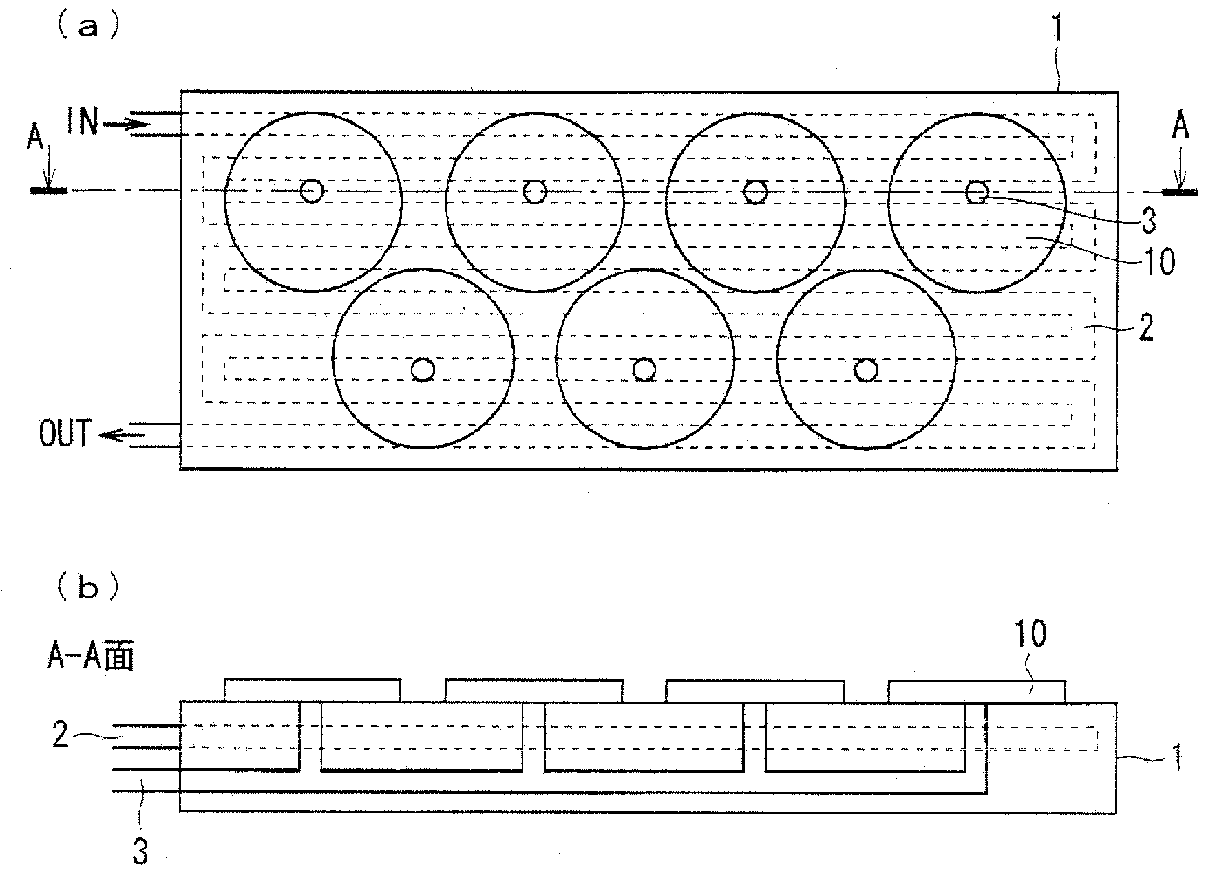
[0039] figure 1 is a block diagram of a semiconductor wafer cooling device according to Embodiment 1, figure 1 (a) is a floor plan, figure 1 (b) is figure 1 A-A section view in (a).
[0040] In the semiconductor wafer cooling device of the present embodiment, a plurality of semiconductor wafers 10 are placed on the tray 1 on the placement surface thereof. A cooling duct 2 is formed inside the tray 1 , and the semiconductor wafer 10 is cooled by a cooling medium such as cooling water flowing through the cooling duct 2 . For example, cooling duct 2 such as figure 1 As shown in (a), one cooling duct is arranged in a folded shape (serpentine arrangement) between both ends of the tray 1 .
[0041] Furthermore, a vacuum duct 3 is formed inside the tray 1 so as not to interfere with the cooling duct 2 , and an opening of the vacuum duct 3 is formed on the mounting surface of the tray 1 . The inside of the vacuum duct 3 is depressurized by a vacuum pump, and the semiconductor wa...
Embodiment approach 2
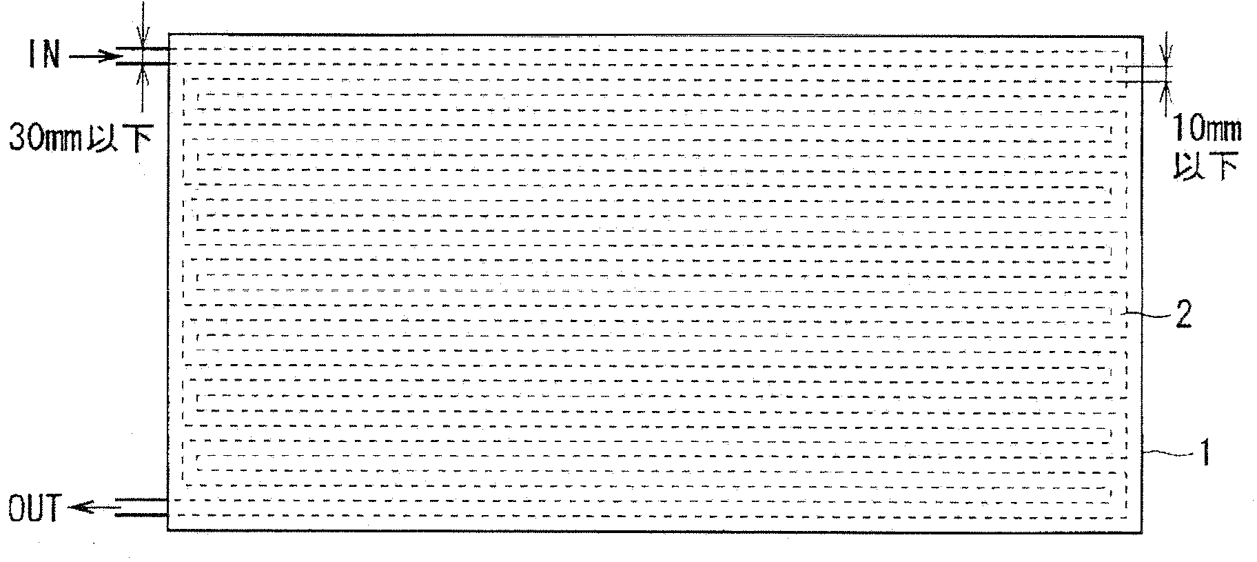
[0047] figure 2 It is a block diagram of the semiconductor wafer cooling apparatus of Embodiment 2. In the semiconductor wafer cooling device of the present embodiment, a plurality of semiconductor wafers 10 are placed on the loading surface of the tray 1 (see figure 1 ). A cooling duct 2 is formed inside the tray 1 , and the semiconductor wafer 10 is cooled by a cooling medium such as cooling water flowing through the cooling duct 2 . The cooling duct 2 is a single cooling duct arranged in a meandering manner (serpentine arrangement) between both ends of the tray 1 .
[0048] When one side of a square chip cut out from the semiconductor wafer 10 is defined as a (mm), and the side wall thickness of the cooling duct 2 is defined as b (mm), the distance between adjacent ducts of the cooling duct 2 ( Pipe interval) c (mm) satisfies:
[0049] [Formula 2]
[0050] c a 2 - 2 b . ...
Embodiment approach 3
[0056] image 3 , Figure 4 It is a block diagram of the semiconductor wafer cooling apparatus of Embodiment 3. In the semiconductor wafer cooling device of the present embodiment, a plurality of semiconductor wafers 10 are placed on the loading surface of the tray 1 (see figure 1 ). A pair of cooling ducts 2a, 2b are formed inside the tray 1, and the semiconductor wafer 10 is cooled by a cooling medium such as cooling water flowing in opposite directions through the cooling ducts 2a, 2b.
[0057] The cooling ducts 2a and 2b each have a structure in which a plurality of branch ducts are connected in parallel, and the branch ducts of the cooling duct 2a and the branch ducts of the cooling duct 2b are alternately arranged on a plane parallel to the mounting surface of the tray 1 .
[0058] Figure 4 (a) is the figure which looked at the cooling duct 2a, 2b from the back side of the tray 1 (the surface opposite to a mounting surface), Figure 4 (b) is from Figure 4 (a) A s...
PUM
 Abstract
Description
Claims
Application Information
 - R&D Engineer
- R&D Manager
- IP Professional
- Industry Leading Data Capabilities
- Powerful AI technology
- Patent DNA Extraction
Browse by: Latest US Patents, China's latest patents, Technical Efficacy Thesaurus, Application Domain, Technology Topic, Popular Technical Reports.
© 2024 PatSnap. All rights reserved.Legal|Privacy policy|Modern Slavery Act Transparency Statement|Sitemap|About US| Contact US: help@patsnap.com


