
Method for forming self-aligned metal silicide

A metal silicide, metal silicide layer technology, applied in electrical components, semiconductor/solid-state device manufacturing, semiconductor devices, etc., can solve problems affecting surface uniformity, unavoidable, metal silicide morphology defects, etc., to improve Interface states, repairs and defects, effects of reducing or avoiding surface defects

Inactive Publication Date: 2015-02-18
SHANGHAI HUALI MICROELECTRONICS CORP
View PDF4 Cites 0 Cited by
  • Summary
  • Abstract
  • Description
  • Claims
  • Application Information

AI Technical Summary

Problems solved by technology

Although the self-aligned metal silicide obtained by the above-mentioned existing manufacturing process can prevent the metal layer from being oxidized to a certain extent through a protective layer such as titanium nitride, it is still unavoidable that a trace amount of oxygen in the reaction atmosphere comes into contact with the generated oxygen during the process. Metal silicide surface, and make it oxidized, resulting in metal silicide morphology defects (such as pyramids), affecting surface uniformity; and the existing process is also prone to defects at the interface between metal silicide and silicon substrate

Method used


Image

  • Method for forming self-aligned metal silicide
  • Method for forming self-aligned metal silicide
  • Method for forming self-aligned metal silicide

Examples


Embodiment Construction

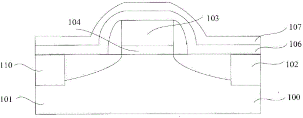
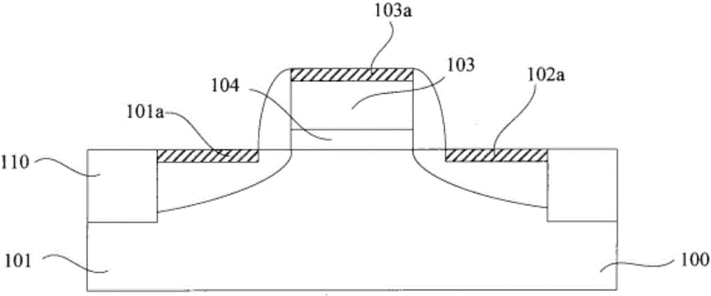
[0031] Embodiments of the present invention use the existing commonly used Ni as the material for forming metal silicides, and are based on a two-step annealing process, combining Figure 4 to Figure 5 , to explain the improvement of the technical solution of the present invention in detail, but the technical solution of the present invention is not limited thereto.

[0032] The method for forming the salicide of this embodiment includes the following steps:

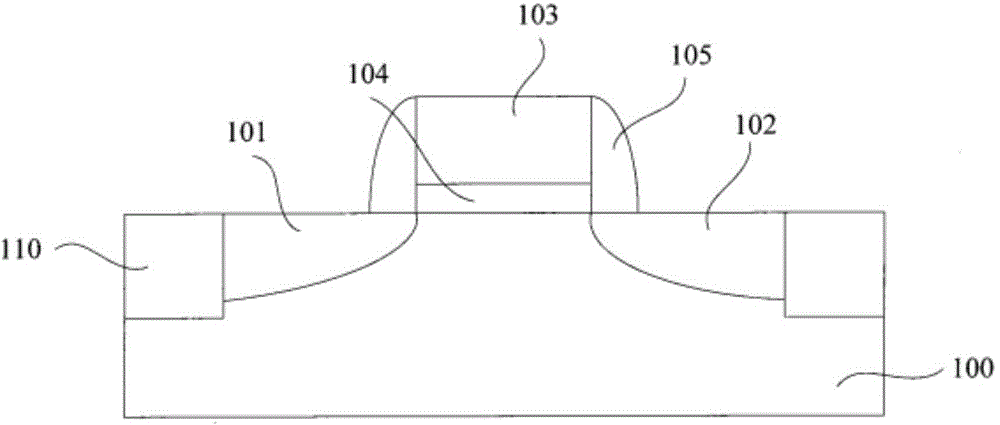
[0033] Step 1, such as Figure 4 As shown, a semiconductor substrate 11 is provided. The surface of the substrate 11 has a silicon region, and the silicon region includes a gate 12 of a MOS transistor and a source region 13 and a drain region 14 formed in the substrate 11 on both sides of the gate 12 . The gate 12 includes a gate dielectric layer 121 , a gate electrode layer 122 , and spacers 123 formed on both sides of the gate dielectric layer and the gate electrode layer.

[0034] Before depositing the metal layer, ...


PUM


Abstract

The invention discloses a method for forming self-aligned metal silicide. The method has the advantages that double-step annealing processes are implemented, hydrogen is introduced in the second annealing process, the hydrogen and trace oxygen in atmosphere react with each other, accordingly, the oxygen can be eliminated, the metal silicide can be prevented from being oxidized, surface defects (such as pyramid shapes) of the metal silicide can be reduced or prevented, and the metal silicide which has flat morphology and is excellent in uniformity can be formed; H atoms in the introduced hydrogen can enter interfaces of the metal silicide and a silicon substrate, and Si-H keys can be formed, so that defects at the interfaces can be repaired and reduced, and interface states (Dit) can be improved.

Description

technical field [0001] The invention relates to the technical field of semiconductor manufacturing, in particular to a method for forming a self-aligned metal silicide. Background technique [0002] In semiconductor manufacturing technology, metal silicide is widely used in source / drain contacts and gate contacts to reduce contact resistance due to its low resistivity and good adhesion with other materials. Metals with high melting points react with silicon to form metal silicides, and metal silicides with low resistivity can be formed through one-step or multi-step annealing process. Early TiSi 2 Due to its narrow line effect, it is no longer suitable for 0.18um technology, and it is used by CoSi 2 replace. CoSi 2 Forming silicide with the same thickness needs to consume more polysilicon or silicon substrates, which can no longer meet the needs of source-drain shallow junctions and ultra-shallow junctions; CoSi 2 On the polysilicon line below 45nm, it shows obvious nar...

Claims


Application Information

Patent Timeline
Patent Type & Authority Applications(China)
IPC IPC(8): H01L21/28H01L21/336
CPCH01L21/28
Inventor 肖天金
Owner SHANGHAI HUALI MICROELECTRONICS CORP
Learn More