


Quick Research
Generate reliable direction feasibility study reports for your R&D in just a few steps.

Technical Q&A
Discover and master advanced knowledge NOW. Basics, ideas, possibilities, all at once.

Find Solutions
As an expert in R&D theories, this can generate solutions to your technical problems instantly.

Evaluate Feasibility
Analyze your overall solution with one click, know your potential R&D risks in advance.

Monitor Landscape
Get weekly tech updates, stay abreast of the latest tech innovations and key insights.
Five-side packaged CSP (chip scale package) structure and manufacturing process
A manufacturing process and bread technology, which is applied in the field of CSP structure and manufacturing process of five-sided packaging, can solve problems such as reliability risks, and achieve the effect of simple manufacturing process and improved reliability
- Summary
- Abstract
- Description
- Claims
- Application Information
AI Technical Summary
Problems solved by technology
Method used
Image

Examples
Embodiment 1
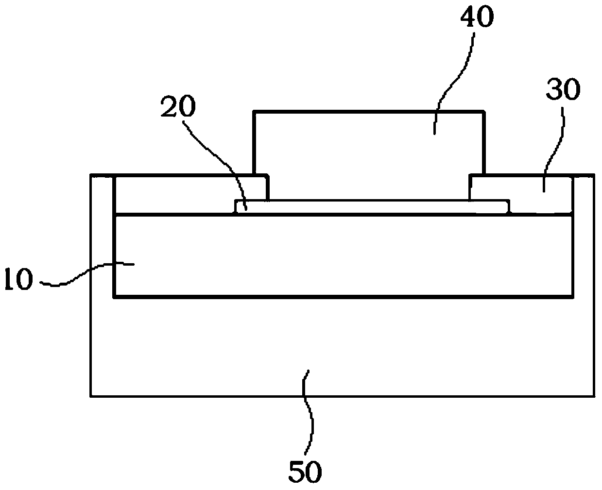
[0030] see figure 1 , a five-sided encapsulation CSP structure given in the figure, including a crystal grain 10 and a pad 20 attached to the surface of the crystal 10, a passivation layer 30 and a conductor 40 attached to the pad 20, the passivation The layer 30 covers the area on the upper surface of the crystal grain 10 that is not covered by the pad 20 and the passivation layer 30 also covers the area of the pad 20 that is not covered by the conductor 40, the bottom surface of the crystal grain 10 and the surrounding sides and passivation layer 30. The surrounding sides of the layer 30 are encapsulated by epoxy resin 50 .
[0031] The manufacturing process of the tube core of this embodiment specifically includes the following steps:
[0032] 1) Prepare the wafer;
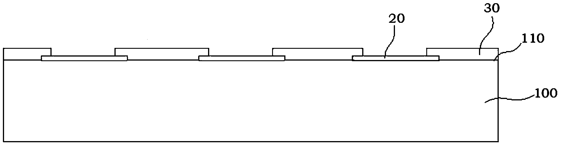
[0033] 2) see figure 2 , on the first surface 110 of the wafer 100, a plurality of welding pads 20 and passivation layers 30 for packaging and bonding are attached at intervals, wherein the passivation la...
Embodiment 2
[0042] see Figure 10 , a five-sided encapsulation CSP structure given in the figure, including a crystal grain 10 and a pad 20 attached to the surface of the crystal 10, a passivation layer 30 and a conductor 40 attached to the pad 20, the passivation The layer 30 covers the area on the upper surface of the crystal grain 10 that is not covered by the pad 20 and the passivation layer 30 also covers the area of the pad 20 that is not covered by the conductor 40 , and a metallization layer is provided on the back of the grain 10 60 , the bottom surface of the metallization layer 60 , the surrounding sides of the crystal grain 10 and the surrounding sides of the passivation layer 30 are encapsulated by the epoxy resin 50 .
[0043] The manufacturing process of the tube core of this embodiment specifically includes the following steps:
[0044] 1) Prepare the wafer;
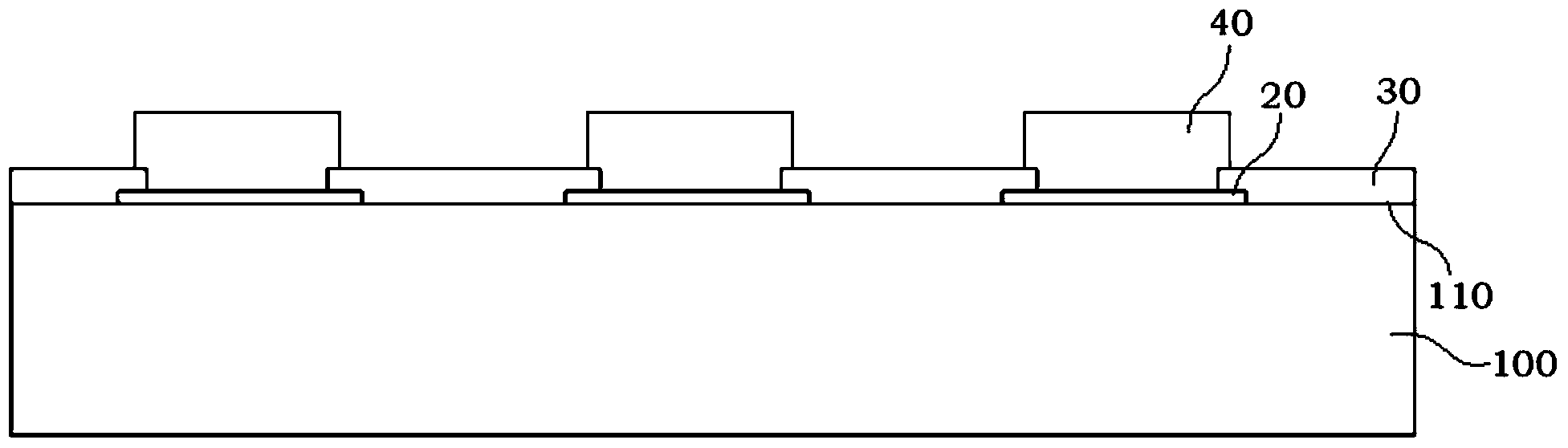
[0045] 2) see Figure 11 , on the first surface 110 of the wafer 100, a plurality of welding pads 20 and pass...
PUM
 Abstract
Description
Claims
Application Information
 - R&D Engineer
- R&D Manager
- IP Professional
- Industry Leading Data Capabilities
- Powerful AI technology
- Patent DNA Extraction
Browse by: Latest US Patents, China's latest patents, Technical Efficacy Thesaurus, Application Domain, Technology Topic, Popular Technical Reports.
© 2024 PatSnap. All rights reserved.Legal|Privacy policy|Modern Slavery Act Transparency Statement|Sitemap|About US| Contact US: help@patsnap.com