


Quick Research
Generate reliable direction feasibility study reports for your R&D in just a few steps.

Technical Q&A
Discover and master advanced knowledge NOW. Basics, ideas, possibilities, all at once.

Find Solutions
As an expert in R&D theories, this can generate solutions to your technical problems instantly.

Evaluate Feasibility
Analyze your overall solution with one click, know your potential R&D risks in advance.

Monitor Landscape
Get weekly tech updates, stay abreast of the latest tech innovations and key insights.
Liquid crystal display element and manufacturing method therefor
A technology of liquid crystal display element and manufacturing method, applied in the direction of instruments, optics, nonlinear optics, etc., to achieve the effect of suppressing the decline of display quality
- Summary
- Abstract
- Description
- Claims
- Application Information
AI Technical Summary
Problems solved by technology
Method used
Image


Examples
Embodiment approach 1
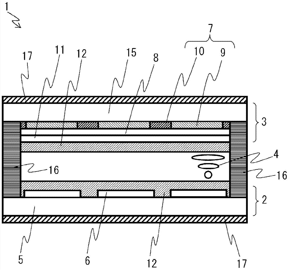
[0073] The liquid crystal display element of Embodiment 1 of this invention is demonstrated using drawing.
[0074] As an example, the liquid crystal display element of the present embodiment may be a TN (Twisted Nematic) type color liquid crystal display element.
[0075] In this case, the liquid crystal display element of this embodiment has, for example, a TFT substrate on which thin film transistors (Thin Film Transistor: TFT) are disposed and a CF substrate having a color filter layer (hereinafter, sometimes referred to as a CF layer). A liquid crystal layer is held, and a sealing material is placed around the pixel formation area where image formation is performed, and these substrates are fixed together.
[0076] Hereinafter, the structure of the liquid crystal display element of this embodiment is demonstrated in more detail.
[0077] figure 1 It is a cross-sectional view schematically showing the structure of the liquid crystal display element of this embodiment.
...
Embodiment approach 2
[0253] Like the liquid crystal display element of Embodiment 1 mentioned above, the liquid crystal display element of Embodiment 2 of this invention is comprised using the liquid crystal aligning film which can reduce performance deterioration effectively even if it receives ultraviolet-ray irradiation. Moreover, in the case of the liquid crystal display element of Embodiment 2, this liquid crystal aligning film is a photo-aligning film which exhibits liquid-crystal orientation control ability by performing photo-alignment process by ultraviolet-ray irradiation. Therefore, the liquid crystal display element according to Embodiment 2 of the present invention is a liquid crystal display element in which reduction in performance degradation is suppressed through a process of irradiating ultraviolet rays in the pixel formation region of the liquid crystal aligning film for photo-alignment treatment.
[0254] The liquid crystal display element of the present embodiment is the same a...
Embodiment approach 3
[0271] The liquid crystal display element according to Embodiment 3 of the present invention is a PSA (Polymer Sustained Alignment) type liquid crystal display element. When constituting a PSA system liquid crystal display element, a vertical alignment type liquid crystal aligning film is used as a liquid crystal aligning film.
[0272] Therefore, it is preferable to form the liquid crystal aligning film of the liquid crystal display element of Embodiment 3 similarly to the liquid crystal aligning film of the liquid crystal display element of Embodiment 1 using a liquid crystal aligning agent. Therefore, the liquid crystal aligning film of the present embodiment preferably uses the liquid crystal aligning agent of the above-mentioned Embodiment 1 in order to provide the liquid crystal display element of the present embodiment in which performance degradation is suppressed through the step of irradiating ultraviolet rays in the pixel forming region. to form. And, in particular...
PUM
| Property | Measurement | Unit |
|---|---|---|
| wavelength | aaaaa | aaaaa |
Abstract
Description
Claims
Application Information
 - R&D Engineer
- R&D Manager
- IP Professional
- Industry Leading Data Capabilities
- Powerful AI technology
- Patent DNA Extraction
Browse by: Latest US Patents, China's latest patents, Technical Efficacy Thesaurus, Application Domain, Technology Topic, Popular Technical Reports.
© 2024 PatSnap. All rights reserved.Legal|Privacy policy|Modern Slavery Act Transparency Statement|Sitemap|About US| Contact US: help@patsnap.com