PUF circuit based on threshold deviation delay
A delay circuit and deviation technology, applied in the field of physical unclonable function circuits, can solve problems such as high cost and inability to be reconfigured
- Summary
- Abstract
- Description
- Claims
- Application Information
AI Technical Summary
Problems solved by technology
Method used
Image
Examples
Embodiment 1
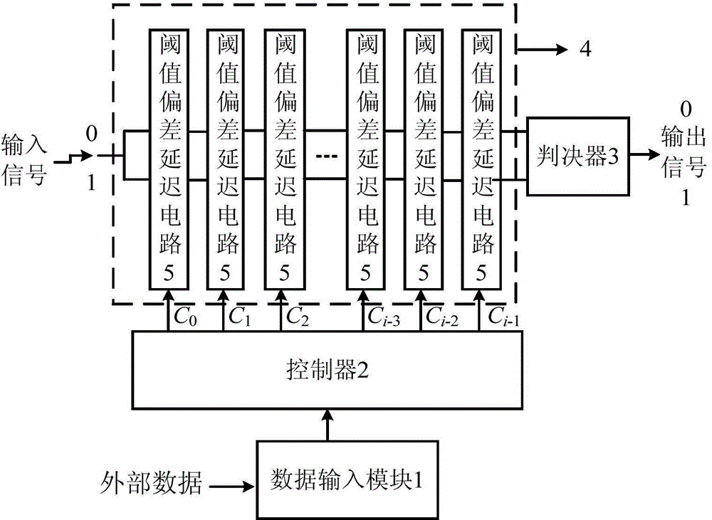
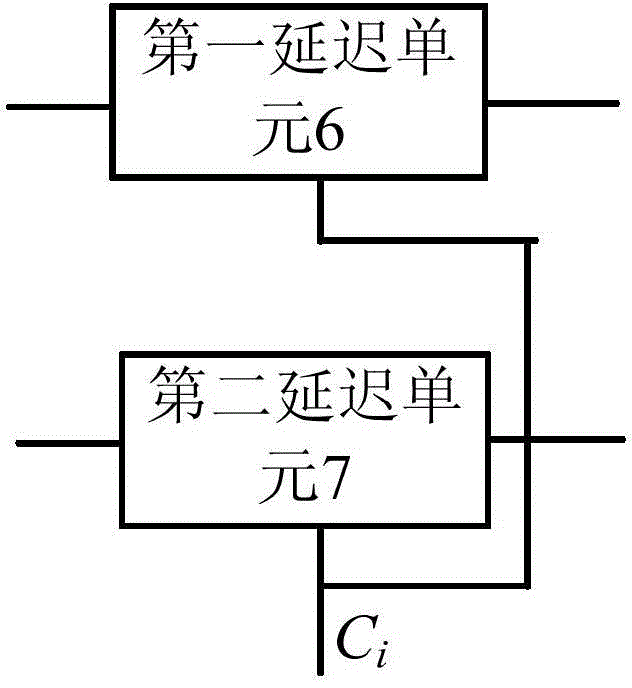
[0020] Embodiment one: if figure 1 and figure 2 As shown, a physical unclonable function circuit based on threshold deviation delay includes a data input module 1, a controller 2, a decision device 3 and a PUF unit circuit 4. The input terminal of the data input module 1 is connected to external data, and the data input module The output end of 1 is connected with the input end of controller 2, and PUF unit circuit 4 comprises i-bit threshold value deviation delay circuit 5, and threshold value deviation delay circuit 5 is made up of two delay units, and two delay units are respectively first delay unit 6 and second delay unit 7;
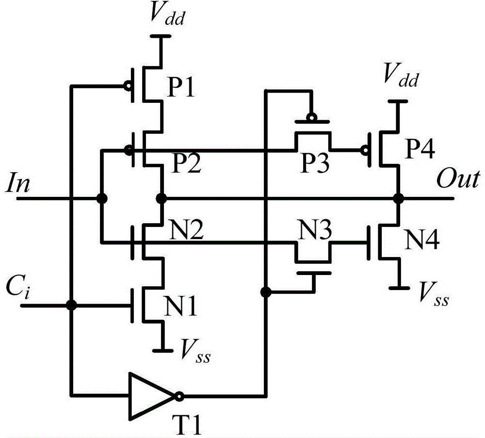
[0021] like image 3 As shown, the delay unit includes a first PMOS transistor P1, a second PMOS transistor P2, a third PMOS transistor P3, a fourth PMOS transistor P4, a first NMOS transistor N1, a second NMOS transistor N2, a third NMOS transistor N3, a fourth The NMOS transistor N4 and the inverter, the source of the first PMOS transistor P1 ...
Embodiment 2
[0032] Embodiment 2: This embodiment is basically the same as Embodiment 1, the only difference is that in this embodiment, the decision device 3 includes a fifth PMOS transistor P5, a sixth PMOS transistor P6, a fifth NMOS transistor N5, a sixth NMOS transistor N6, The seventh NMOS transistor N7 and the eighth NMOS transistor N8, the source of the fifth PMOS transistor P5 and the source of the sixth PMOS transistor P6 are connected to the power supply, the drain of the fifth PMOS transistor P5, the drain of the fifth NMOS transistor N5 pole, the drain of the sixth NMOS transistor N6, the gate of the sixth PMOS transistor P6 and the gate of the seventh NMOS transistor N7 are connected, the gate of the fifth PMOS transistor P5, the gate of the sixth NMOS transistor N6, the gate of the sixth NMOS transistor N6 The drain of the PMOS transistor P6, the drain of the seventh NMOS transistor N7 and the drain of the eighth NMOS transistor N8 are connected and the connection end is the ...
PUM
 Abstract
Description
Claims
Application Information
 - R&D
- Intellectual Property
- Life Sciences
- Materials
- Tech Scout
- Unparalleled Data Quality
- Higher Quality Content
- 60% Fewer Hallucinations
Browse by: Latest US Patents, China's latest patents, Technical Efficacy Thesaurus, Application Domain, Technology Topic, Popular Technical Reports.
© 2025 PatSnap. All rights reserved.Legal|Privacy policy|Modern Slavery Act Transparency Statement|Sitemap|About US| Contact US: help@patsnap.com


