
Selectable error amplifier and voltage comparator multiplex circuit

A voltage comparator and error amplifier technology, applied in the field of analog integrated circuit design, can solve the problems of reducing chip area, the contradiction between chip area and conversion efficiency, and reducing the complexity of circuit design, so as to reduce complexity, solve the problem of chip area and conversion Efficiency has paradoxical effects

Active Publication Date: 2014-11-05
XIDIAN UNIV
View PDF8 Cites 5 Cited by
  • Summary
  • Abstract
  • Description
  • Claims
  • Application Information

AI Technical Summary

Problems solved by technology

[0003] The purpose of the present invention is to provide a selectable error amplifier and voltage comparator multiplexing circuit, which solves the problem of conflict between chip area and conversion efficiency in the multi-mode modulation DC-DC converter circuit, and reduces the complexity of circuit design degree, and effectively reduce the chip area

Method used


Image

  • Selectable error amplifier and voltage comparator multiplex circuit
  • Selectable error amplifier and voltage comparator multiplex circuit
  • Selectable error amplifier and voltage comparator multiplex circuit

Examples


Embodiment Construction

[0035] In order to make the technical problems, technical solutions and advantages to be solved by the present invention clearer, the following will describe in detail with reference to the drawings and specific embodiments.

[0036] The present invention aims at the problem that there is a contradiction between the chip area and conversion efficiency in the multi-mode modulation DC-DC converter circuit in the prior art, and provides an optional error amplifier and voltage comparator multiplexing circuit, which is realized by a control signal The selection of circuit function, the input stage load circuit and the error amplifier output circuit constitute the error amplifier structure, which works when the control signal is high level; the input stage load circuit and the voltage comparator output circuit constitute the comparator structure, when the control signal is low work at the same level; at the same time, the multiplexing circuit is applied to the multi-mode modulation D...


PUM


Abstract

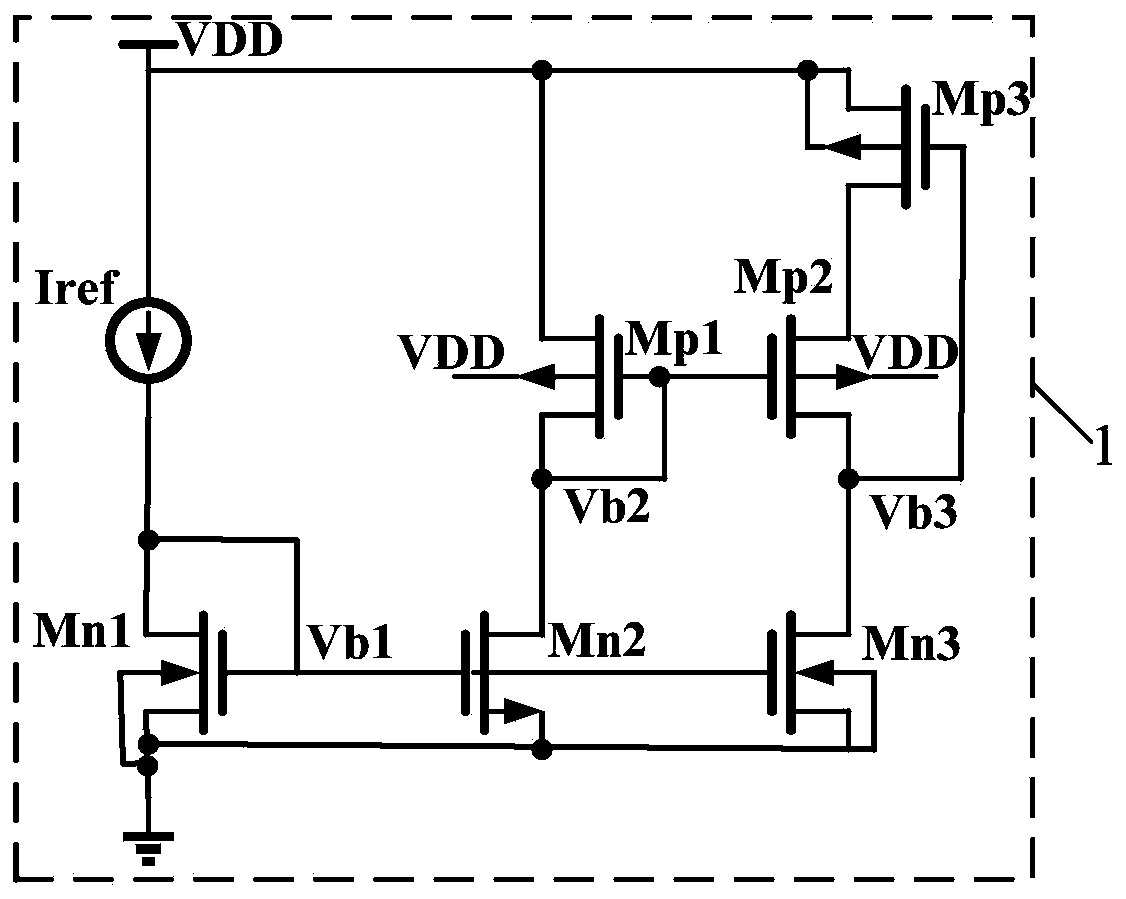
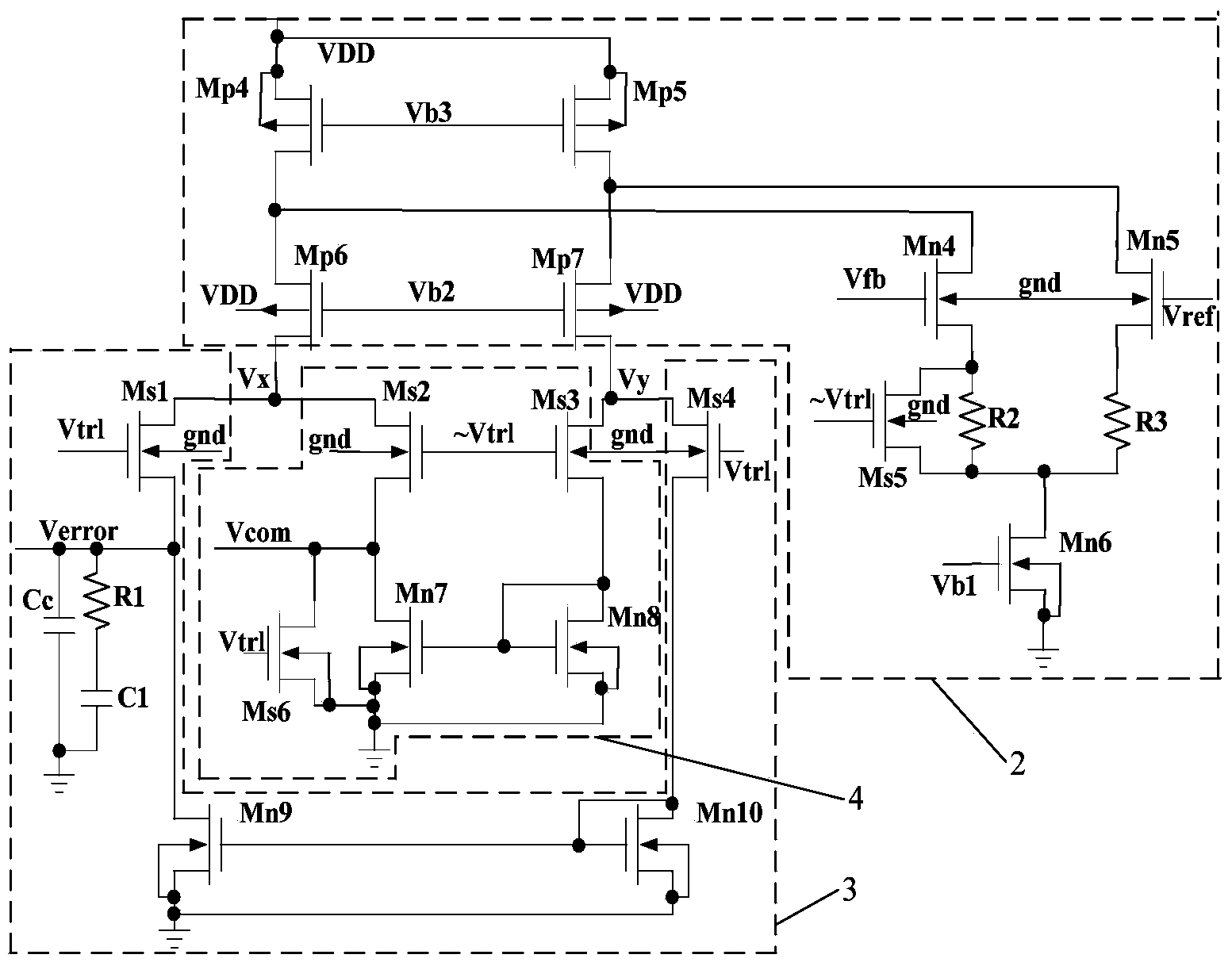
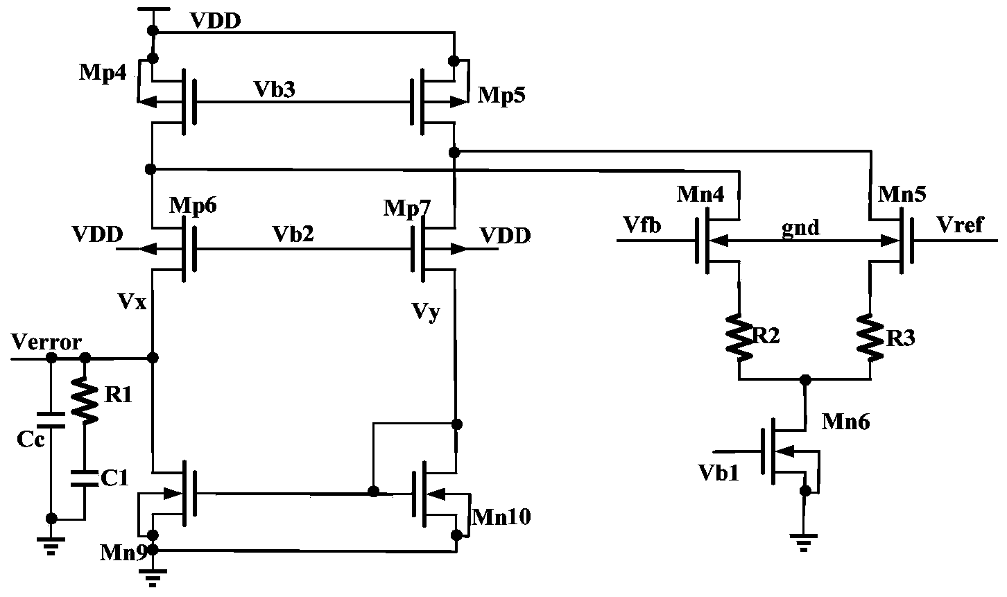
The invention provides a selectable error amplifier and voltage comparator multiplex circuit. The multiplex circuit comprises a bias voltage generation circuit, an input stage load circuit, an error amplifier output circuit and a voltage comparator output circuit, wherein the bias voltage generation circuit provides a bias voltage for the input stage load circuit, the output end of the input stage load circuit is connected with the error amplifier output circuit and the voltage comparator output circuit, and the error amplifier output circuit or the voltage comparator output circuit is gated through a control signal. According to the multiplex circuit, selection of circuit functions is achieved through the control signal, the input stage load circuit and the error amplifier output circuit form an error amplifier structure, and when the control signal is at a low level, the input stage load circuit and the voltage comparator output circuit form a comparator structure. When applied to a multi-model modulation type DC-DC converter circuit, the multiplex circuit removes the conflict between the chip area and the conversion efficiency of the converter circuit.

Description

technical field [0001] The invention relates to the field of analog integrated circuit design, in particular to a selectable error amplifier and voltage comparator multiplexing circuit. Background technique [0002] In order to make the DC-DC converter have higher conversion efficiency in a wide load range, it is necessary to enable the converter to automatically adopt different modulation modes according to the load conditions. Currently the most commonly used modulation modes are Pulse Width Modulation (PWM) and Burst (BURST) modes. Pulse width modulation (PWM) means that the power tube pulse control signal has a constant duty cycle, so that a stable voltage can be output; intermittent (BURST) modulation mode refers to several consecutive clock cycles of the converter control circuit within time t Output pulse signal to control the power tube to work, and output low level at other times to keep the power tube in cut-off state. In the working phase of the power tube, the ...

Claims


Application Information

Patent Timeline
IPC IPC(8): H02M3/00
Inventor 刘帘曦宋宇马丽张雪军朱樟明杨银堂
Owner XIDIAN UNIV
Learn More